CLOCK5xoy.com
5xoy.com 时间:2021-03-19 阅读:()
a5VCATVLineDriverFineStepOutputPowerControlAD8325FEATURESFUNCTIONALBLOCKDIAGRAMSupportsDOCSISStandardforReversePathVCC(7PINS)BYPTransmissionGainProgrammablein0.
75dBStepsOvera59.
45dBRangeLowDistortionat61dBmVOutputVIN+–57dBcSFDRat21MHzDIFFORSINGLEINPUTAMPATTENUATIONCOREZOUTDIFF=75888ZIN(SINGLE)=800ZIN(DIFF)=1.
6kR1R2AD8325VERNIERDECODEDATALATCHSHIFTREGISTERPOWER-DOWNLOGICPOWERAMPOutputNoiseLevel–48dBmVin160kHzMaintains75OutputImpedanceTransmitEnableandTransmitDisableModesUpperBandwidth:100MHz(FullGainRange)5VSupplyOperationSupportsSPIInterfacesAPPLICATIONSGain-ProgrammableLineDriver–55dBcSFDRat42MHzVIN–VOUT+VOUT–DOCSISHigh-SpeedDataModemsInteractiveCableSet-TopBoxesPCPlug-inCableModemsGeneral-PurposeDigitallyControlledVariableGainBlockGENERALDESCRIPTIONTheAD8325isalow-cost,digitallycontrolled,variablegainamplifieroptimizedforcoaxiallinedrivingapplicationssuchascablemodemsthataredesignedtotheMCNS-DOCSISupstream–50standard.
An8-bitserialworddeterminesthedesiredoutputgainovera59.
45dBrangeresultingingainchangesof0.
7526dB/LSB.
–52TheAD8325comprisesadigitallycontrolledvariableattenuator–54of0dBto–59.
45dB,whichisprecededbyalownoise,fixedgainbufferandisfollowedbyalowdistortionhighpoweramplifier.
TheAD8325acceptsadifferentialorsingle-endedinputsignal.
Theoutputisspecifiedfordrivinga75Wload,suchascoaxialcable.
DISTORTION–dBc–56–58Distortionperformanceof–57dBcisachievedwithanoutput–60levelupto61dBmVat21MHzbandwidth.
Akeyperformance–62andcostadvantageoftheAD8325resultsfromtheabilitytomaintainaconstant75WoutputimpedanceduringTransmit–64DATENDATACLKGND(11PINS)TXENSLEEPVOUTVOUT=62dBmV@MAXGAIN=61dBmV@MAXGAINVOUT=60dBmV@MAXGAINVOUT=59dBmV@MAXGAINEnableandTransmitDisableconditions.
Inaddition,this51525354555devicehasasleepmodefunctionthatreducesthequiescentFUNDAMENTALFREQUENCY–MHzcurrentto4mA.
Figure1.
WorstHarmonicDistortionvs.
GainControlTheAD8325ispackagedinalow-cost28-leadTSSOP,operatesfromasingle5Vsupply,andhasanoperationaltemperaturerangeof–40∞Cto+85∞C.
REV.
AInformationfurnishedbyAnalogDevicesisbelievedtobeaccurateandreliable.
However,noresponsibilityisassumedbyAnalogDevicesforitsuse,norforanyinfringementsofpatentsorotherrightsofthirdpartiesthatmayresultfromitsuse.
NolicenseisgrantedbyimplicationorotherwiseOneTechnologyWay,P.
O.
Box9106,Norwood,MA02062-9106,U.
S.
A.
underanypatentorpatentrightsofAnalogDevices.
TrademarksandTel:781/329-4700www.
analog.
comregisteredtrademarksarethepropertyoftheirrespectiveowners.
Fax:781/461-31132005AnalogDevices,Inc.
Allrightsreserved.
65AD8325*PRODUCTPAGEQUICKLINKSLastContentUpdate:02/23/2017COMPARABLEPARTSViewaparametricsearchofcomparableparts.
DOCUMENTATIONApplicationNotesAN-851:AWiMaxDoubleDownconversionIFSamplingReceiverDesignDataSheetAD8325:5VCATVLineDriverFineStepOutputPowerControlDataSheetREFERENCEMATERIALSProductSelectionGuideVariableGainAmplifierSelectionTableTutorialsDesignandOperationofAutomaticGainControlLoopsforReceiversinModernCommunicationSystemsDESIGNRESOURCESAD8325MaterialDeclarationPCN-PDNInformationQualityAndReliabilitySymbolsandFootprintsDISCUSSIONSViewallAD8325EngineerZoneDiscussions.
SAMPLEANDBUYVisittheproductpagetoseepricingoptions.
TECHNICALSUPPORTSubmitatechnicalquestionorfindyourregionalsupportnumber.
DOCUMENTFEEDBACKSubmitfeedbackforthisdatasheet.
ThispageisdynamicallygeneratedbyAnalogDevices,Inc.
,andinsertedintothisdatasheet.
Adynamicchangetothecontentonthispagewillnottriggerachangetoeithertherevisionnumberorthecontentoftheproductdatasheet.
Thisdynamicpagemaybefrequentlymodified.
AD8325–SPECIFICATIONS(TA=25C,VS=5V,RL=75,VIN(differential)=31dBmV,VOUTmeasuredthrougha1:1transformer1withaninsertionlossof0.
5dB@10MHzunlessotherwisenoted.
)ParameterConditionsMinTypMaxUnitINPUTCHARACTERISTICSSpecifiedACVoltageOutput=61dBmV,MaxGain31dBmVNoiseFigureMaxGain,f=10MHz13.
8dBInputResistanceSingle-EndedInput800WDifferentialInput1600WInputCapacitance2pFGAINCONTROLINTERFACEGainRange58.
4559.
4560.
45dBMaximumGainGainCode=79Dec29.
230.
030.
8dBMinimumGainGainCode=0Dec–30.
25–29.
45–28.
65dBGainScalingFactor0.
7526dB/LSBOUTPUTCHARACTERISTICSBandwidth(–3dB)BandwidthRoll-OffAllGainCodesf=65MHz1001.
6MHzdBBandwidthPeakingOutputNoiseSpectralDensityf=65MHzMaxGain,f=10MHz0–33dBdBmVin160kHzMinGain,f=10MHz–48dBmVin160kHzTransmitDisableMode,f=10MHz–68dBmVin160kHz1dBCompressionPointDifferentialOutputImpedanceMaxGain,f=10MHzTransmitEnableandTransmitDisableModes18.
575±20%dBmWOVERALLPERFORMANCESecondOrderHarmonicDistortionf=21MHz,VOUT=61dBmV@MaxGain–70dBcf=42MHz,VOUT=61dBmV@MaxGain–67dBcf=65MHz,VOUT=61dBmV@MaxGain–60dBcThirdOrderHarmonicDistortionf=21MHz,VOUT=61dBmV@MaxGain–57dBcf=42MHz,VOUT=61dBmV@MaxGain–55dBcf=65MHz,VOUT=61dBmV@MaxGain–54dBcAdjacentChannelPowerAdjacentChannelWidth=TransmitChannel–53.
8dBcGainLinearityErrorWidth=160KSYM/SECf=10MHz,CodetoCode±0.
3dBOutputSettlingDuetoGainChange(TGS)MintoMaxGain60nsDuetoInputChangeMaxGain,VIN=31dBmV30nsIsolationinTransmitDisableModeMaxGain,TXEN=0V,f=42MHz,–33dBcVIN=31dBmVPOWERCONTROLTransmitEnableSettlingTime(TON)MaxGain,VIN=0V300nsTransmitDisableSettlingTime(TOFF)MaxGain,VIN=0V40nsBetweenBurstTransients2EquivalentOutput=31dBmV3mVp-pEquivalentOutput=61dBmV50mVp-pPOWERSUPPLYOperatingRange4.
7555.
25VQuiescentCurrentTransmitEnableMode(TXEN=1)123133140mATransmitDisableMode(TXEN=0)303510mASleepMode247mAOPERATINGTEMPERATURERANGE–40+85∞CNOTES1TOKO617DB-A0070usedforabovespecifications.
MACOMETC-1-IT-15canbesubstituted.
2BetweenBurstTransientsmeasuredattheoutputofa42MHzdiplexer.
Specificationssubjecttochangewithoutnotice.
–2–REV.
AAD8325LOGICINPUTS(TTL/CMOS-CompatibleLogic)(DATEN,CLK,SDATA,TXEN,SLEEP,VCC=5V:FullTemperatureRange)ParameterLogic"1"VoltageLogic"0"VoltageLogic"1"Current(VINH=5V)CLK,SDATA,DATENLogic"0"Current(VINL=0V)CLK,SDATA,DATENLogic"1"Current(VINH=5V)TXENLogic"0"Current(VINL=0V)TXENLogic"1"Current(VINH=5V)SLEEPLogic"0"Current(VINL=0V)SLEEPMinTypMaxUnit2.
15.
0V00.
8V020nA–600–100nA50190mA–250–30mA50190mA–250–30mATIMINGREQUIREMENTS(FullTemperatureRange,VCC=5V,TR=TF=4ns,fCLK=8MHzunlessotherwisenoted.
)ParameterMinTypMaxUnitClockPulsewidth(TWH)16.
0nsClockPeriod(TC)32.
0nsSetupTimeSDATAvs.
Clock(TDS)5.
0nsSetupTimeDATENvs.
Clock(TES)15.
0nsHoldTimeSDATAvs.
Clock(TDH)5.
0nsHoldTimeDATENvs.
Clock(TEH)3.
0nsInputRiseandFallTimes,SDATA,DATEN,Clock(TR,TF)10nsTDSSDATACLKDATENTXENANALOGOUTPUTTESVALIDDATAWORDG1MSB.
.
.
.
LSBGAINTRANSFER(G1)TEH8CLOCKCYCLESGAINTRANSFER(G2)TOFFTGSSIGNALAMPLITUDE(p-p)TONTCTWHVALIDDATAWORDG2Figure2.
SerialInterfaceTimingSDATACLKVALIDDATABITMSBMSB-1MSB-2TDSTDHFigure3.
SDATATimingREV.
A–3–AD8325ABSOLUTEMAXIMUMRATINGS*SupplyVoltage+VSPins5,9,10,19,20,23,276VInputVoltagesPins25,260.
5VPins1,2,3,6,70.
8Vto+5.
5VInternalPowerDissipationTSSOP0.
9WOperatingTemperatureRange40∞Cto+85∞CStorageTemperatureRange65∞Cto+150∞CLeadTemperature,Soldering60seconds300∞C*StressesabovethoselistedunderAbsoluteMaximumRatingsmaycausepermanentdamagetothedevice.
Thisisastressratingonly;functionaloperationofthedeviceattheseoranyotherconditionsabovethoseindicatedintheoperationalsectionofthisspecificationisnotimplied.
Exposuretoabsolutemaximumratingconditionsforextendedperiodsmayaffectdevicereliability.
PINCONFIGURATIONTOPVIEW(NottoScale)28272625242322212019181716151234567891011121314AD8325GNDDATENSDATAVCCCLKVIN–GNDVIN+GNDVCCTXENVCCGNDSLEEPGNDBYPVCCVCCVCCVCCGNDGNDGNDGNDGNDGNDOUT–OUT+ORDERINGGUIDEModelTemperatureRangePackageDescriptionJAPackageOptionAD8325ARU–40∞Cto+85∞C28-LeadTSSOP67.
7∞C/W1RU-28AD8325ARU-REEL–40∞Cto+85∞C28-LeadTSSOP67.
7∞C/W1RU-28AD8325ARUZ2–40∞Cto+85∞C28-LeadTSSOP67.
7∞C/W1RU-28AD8325ARUZ-REEL2–40∞Cto+85∞C28-LeadTSSOP67.
7∞C/W1RU-28AD8325-EVALEvaluationBoard1ThermalResistancemeasuredonSEMIstandard4-layerboard.
2Z=Pb-freepart.
CAUTIONESD(electrostaticdischarge)sensitivedevice.
Electrostaticchargesashighas4000Vreadilyaccumulateonthehumanbodyandtestequipmentandcandischargewithoutdetection.
AlthoughtheAD8325featuresproprietaryESDprotectioncircuitry,permanentdamagemayoccurondevicessubjectedtohigh-energyelectrostaticdischarges.
Therefore,properESDprecautionsarerecommendedtoavoidperformancedegradationorlossoffunctionality.
WARNING!
ESDSENSITIVEDEVICEPinNo.
MnemonicDescription1DATENDataEnableLowInput.
Thisportcontrolsthe8-bitparalleldatalatchandshiftregister.
ALogic0-to-1transitiontransfersthelatcheddatatotheattenuatorcore(updatesthegain)andsimultaneouslyinhibitsserialdatatransferintotheregister.
A1-to-0transitioninhibitsthedatalatch(holdsthepreviousgainstate)andsimultaneouslyenablestheregisterforserialdataload.
2SDATASerialDataInput.
Thisdigitalinputallowsforan8-bitserial(gain)wordtobeloadedintotheinternalregisterwiththeMSB(MostSignificantBit)first.
3CLKClockInput.
Theclockportcontrolstheserialattenuatordatatransferratetothe8-bitmaster-slaveregister.
ALogic0-to-1transitionlatchesthedatabitanda1-to-0transfersthedatabittotheslave.
Thisrequirestheinputserialdatawordtobevalidatorbeforethisclocktransition.
4,8,11,12,GNDCommonExternalGroundReference.
13,16,17,18,22,24,285,9,10,19,VCCCommonPositiveExternalSupplyVoltage.
A0.
1mFcapacitormustdecoupleeachpin.
20,23,276TXENLogic"0"disablestransmission.
Logic"1"enablestransmission.
7SLEEPLowPowerSleepMode.
Logic0enablesSleepmode,whereZOUTgoesto400Wandsupplycurrentisreducedto4mA.
Logic1enablesnormaloperation.
14OUT–NegativeOutputSignal.
15OUT+PositiveOutputSignal.
21BYPInternalBypass.
Thispinmustbeexternallyac-coupled(0.
1mFcap).
25VIN+NoninvertingInput.
DC-biasedtoapproximatelyVCC/2.
Shouldbeac-coupledwitha0.
1mFcapacitor.
26VIN–InvertingInput.
DC-biasedtoapproximatelyVCC/2.
Shouldbeac-coupledwitha0.
1mFcapacitor.
PINFUNCTIONDESCRIPTIONS–4–REV.
ATypicalPerformanceCharacteristics–AD83253431VCCTOKO617DB–A0070OUT–OUT+VIN+VIN–GND0.
1F165VIN75RL1:10.
1FAD8325GAIN–dB28252219CL=20pFCL=10pFCL=0pFVOUT=61dBmV@MAXGAINOUT–OUT+GNDVIN+VIN–VIN16575CLRLTOKO617DB–A00701:1VCCCL=50pF0.
1F0.
1F110100FREQUENCY–MHzTPC1.
BasicTestCircuitTPC4.
ACResponseforVariousCapLoads–300.
5f=10MHzf=5MHzf=42MHzf=65MHzf=TXE10MHzN=1OUTPUTNOISE–dBmVIN160kHz–34–38–42–460GAINERROR–dBGAIN–dB–0.
5–1.
0–1.
5010203040506070GAINCONTROL–Decimal–508008162432404856647280GAINCONTROL–Decimal–2.
0TPC2.
GainErrorvs.
GainControlTPC5.
OutputReferredNoisevs.
GainControl00D23D46D79D040TXEN=0VIN=31dBmVMAXGAINMINGAIN30–202010ISOLATION–dB–400–10–60–20–30–80–40–50–1000.
111010010000.
11101001000FREQUENCY–MHzFREQUENCY–MHzTPC3.
ACResponseTPC6.
IsolationinTransmitDisableModevs.
FrequencyREV.
A–5–AD8325–55180170–60–75TXEN=0TXEN=1OUT–OUT+GNDVIN+VIN–165RLTOKO617DB–A00701:1VCC0.
1F0.
1FZIN7551525354555FUNDAMENTALFREQUENCY–MHz11065110100FREQUENCY–MHzTPC7.
SecondOrderHarmonicDistortionvs.
FrequencyTPC10.
InputImpedancevs.
FrequencyforVariousOutputLevels–5090VBmV@MAXGAINVOUT=61dBmV@OUT=62dMAXGAINVOUT=60dBmV@MAXGAINVOUT=59dBmV@MAXGAIN160150DISTORTION–dBcIMPEDANCE–IMPEDANCE––65140130–70120VOUT=62dBmV@MAXGAINVOUT=61dBmV@MAXGAINVOUT=60dBmV@MAXGAINVOUT=59dBmV@MAXGAINTXEN=0TXEN=1–5285–5480DISTORTION–dBc–56–587570–6065–6260–64555152535455565110100FUNDAMENTALFREQUENCY–MHzFREQUENCY–MHzTPC8.
ThirdOrderHarmonicDistortionvs.
FrequencyforTPC11.
OutputImpedancevs.
FrequencyVariousOutputLevels–10–50CHPWR12.
3dBmACPUP–54.
02dBACPLOW–53.
79dBC0C0CU1CU1C11C11FO=VOUT42MHz=61dBmV@MAXGAINHD3HD2–20–30–40–50–60–70–80–90–100–110–55DISTORTION–dBc–60–65–70–75–8001020304050607080CENTER21MHz75kHz/DIVSPAN750kHzGAINCONTROL–DecCodeTPC9.
HarmonicDistortionvs.
GainControlTPC12.
AdjacentChannelPower–6–REV.
AAD8325withatransformer,thestatedgainvaluesalreadytakeintoaccountthelossesassociatedwiththetransformer.
Thegaintransferfunctionisasfollows:AV=30.
0dB–(0.
7526dB(79–CODE))for0CODE79whereAVisthegainindBandCODEisthedecimalequivalentofthe8-bitword.
Validgaincodesarefrom0to79.
Figure4showsthegaincharacteristicsoftheAD8325forallpossiblevaluesinan8-bitword.
NotethatmaximumgainisachievedatCode79.
FromCode80through127,the5.
25dBofattenuationfromthevernierstageisbeingappliedovereveryeightcodes,resultinginthesawtoothcharacteristicatthetopofthegainrange.
Becausetheeighthbitisa"don'tcare"bit,thecharacteristicforcodes0through127repeatsfromCodes128through255.
3025201510APPLICATIONSGeneralApplicationTheAD8325isprimarilyintendedforuseastheupstreampoweramplifier(PA)inDOCSIS(DataOverCableServiceInterfaceSpecifications)certifiedcablemodemsandCATVset-topboxes.
UpstreamdataismodulatedinQPSKorQAMformat,anddonewithDSPoradedicatedQPSK/QAMmodulator.
TheamplifierreceivesitsinputsignalfromtheQPSK/QAMmodulatororfromaDAC.
Ineithercasethesignalmustbelow-passfilteredbeforebeingappliedtotheamplifier.
Becausethedistancefromthecablemodemtothecentralofficewillvarywitheachsubscriber,theAD8325mustbecapableofvaryingitsoutputpowerbyapplyinggainorattenuationtoensurethatallsignalsarrivingatthecentralofficeareofthesameamplitude.
Theupstreamsignalpathcontainscomponentssuchasatransformeranddiplexerthatwillresultinsomeamountofpowerloss.
Therefore,theamplifiermustbecapableofprovidingenoughpowerintoa75Wloadtoovercometheselosseswithoutsacrificingtheintegrityoftheoutputsignal.
OperationalDescriptionTheAD8325iscomposedoffouranalogfunctionsinthepower-uporforwardmode.
Theinputamplifier(preamp)canbeusedsingle-endedlyordifferentially.
Iftheinputisusedinthedifferentialconfiguration,itisimperativethattheinputsignalsare180degreesoutofphaseandofequalamplitudes.
ThiswillensureGAIN–dB50–5propergainaccuracyandharmonicperformance.
Thepreampstagedrivesavernierstagethatprovidesthefinetunegainadjustment.
The0.
7526dBstepresolutionisimplementedinthevernierstageandprovidesatotalofapproximately5.
25dBofattenuation.
Afterthevernierstage,aDACprovidesthebulkoftheAD8325'sattenuation(9bitsor54dB).
ThesignalsinthepreampandverniergainblocksaredifferentialtoimprovethePSRRandlinearity.
AdifferentialcurrentisfedfromtheDACintotheoutputstage,whichamplifiesthesecurrentstotheappropriatelevelsnecessarytodrivea75Wload.
Theoutputstageutilizesnegativefeedbacktoimplementadifferential75Woutputimpedance.
Thiseliminatestheneedforexternalmatchingresistorsneededintypicalvideo(orvideofilter)terminationrequirements.
SPIProgrammingandGainAdjustmentGainprogrammingoftheAD8325isaccomplishedusingaserialperipheralinterface(SPI)andthreedigitalcontrollines,DATEN,SDATA,andCLK.
Tochangethegain,eightbitsofdataarestreamedintotheserialshiftregisterthroughtheSDATAport.
TheSDATAloadsequencebeginswithafallingedgeontheDATENpin,thusactivatingtheCLKline.
WiththeCLKlineactivated,dataontheSDATAlineisclockedintotheserialshiftregisterMostSignificantBit(MSB)first,ontherising–10–15–20–25–300326496128160192224256GAINCODE–DecimalFigure4.
Gainvs.
GainCodeInputBias,Impedance,andTerminationTheVIN+andVIN–inputshaveadcbiaslevelofapproximatelyVCC/2,thereforetheinputsignalshouldbeac-coupled.
Thedifferentialinputimpedanceisapproximately1600Wwhilethesingle-endedinputimpedanceis800W.
IftheAD8325isbeingoperatedinasingle-endedinputconfigurationwithadesiredinputimpedanceof75W,theVIN+andVIN–inputsshouldbeterminatedasshowninFigure5.
Ifaninputimpedanceotherthan75Wisdesired,thevaluesofR1andR2inFigure5canbecalculatedusingthefollowingequations:ZIN=R1800R2=ZINR1ZIN=75edgeofeachCLKpulse.
Becauseonlya7-bitshiftregisterisused,theMSBofthe8-bitwordisa"don'tcare"bitandisshiftedoutoftheregisterontheeighthclockpulse.
ArisingedgeontheDATENlinelatchesthecontentsoftheshiftregisterintotheattenuatorcoreresultinginawellcontrolledchangeintheoutputsignallevel.
TheserialinterfacetimingfortheAD8325isAD8325R1=82.
5R2=39.
2+–Figure5.
Single-EndedInputTerminationshowninFigures2and3.
TheprogrammablegainrangeoftheAD8325is–29.
45dBto+30dBandscales0.
7526dBperleastsignificantbit(LSB).
BecausetheAD8325wascharacterizedREV.
A–7–AD8325OutputBias,Impedance,andTerminationThedifferentialoutputpinsVOUT+andVOUT–arealsobiasedtoadclevelofapproximatelyVCC/2.
Therefore,theoutputsshouldbeac-coupledbeforebeingappliedtotheload.
Thisisaccomplishedwitha1:1transformerasseeninthetypicalapplicationscircuitofFigure6.
Thetransformeralsoconvertstheoutputsignalfromdifferentialtosingle-ended,whilemaintainingaproperimpedancematchtotheline.
ThedifferentialoutputimpedanceoftheAD8325isinternallymaintainedat75W,regardlessofwhethertheamplifierisintransmitenablemode(TXEN=1)ortransmitdisablemode(TXEN=0).
Iftheoutputsignalisbeingevaluatedonstandard50Wtestequipment,a75Wto50Wpadmustbeusedtoprovidethetestcircuitwiththecorrectimpedancematch.
PowerSupplyDecoupling,Grounding,andLayoutConsiderationsCarefulattentiontoprintedcircuitboardlayoutdetailswillpreventproblemsduetoassociatedboardparasitics.
ProperRFdesigntechniquesaremandatory.
The5VsupplypowershouldbedeliveredtoeachoftheVCCpinsviaalowimpedancepowerbustoensurethateachpinisatthesamepotential.
Thepowerbusshouldbedecoupledtogroundwitha10mFtantalumcapacitorlocatedincloseproximitytotheAD8325.
Inadditiontothe10mFcapacitor,eachVCCpinshouldbeindividuallydecoupledtogroundwitha0.
1mFceramicchipcapacitorlocatedasclosetothepinaspossible.
ThepinlabeledBYP(Pin21)shouldalsobedecoupledwitha0.
1mFcapacitor.
ThePCBshouldhavealow-impedancegroundplanecoveringallunusedportionsofthecomponentsideoftheboard,exceptintheareaoftheinputandoutputtraces(seeFigure10).
ItisimportantthatalloftheAD8325'sgroundpinsareconnectedtothegroundplanetoensurepropergroundingofallinternalnodes.
Thedifferential5VTXENSLEEPinputandoutputtracesshouldbekeptasshortandsymmetricalaspossible.
Inaddition,theinputandoutputtracesshouldbekeptfarapartinordertominimizecoupling(crosstalk)throughtheboard.
FollowingtheseguidelineswillimprovetheoverallperformanceoftheAD8325inallapplications.
InitialPower-UpWhenthe5VsupplyisfirstappliedtotheVCCpinsoftheAD8325,thegainsettingoftheamplifierisindeterminate.
Therefore,aspowerisfirstappliedtotheamplifier,theTXENpinshouldbeheldlow(Logic0)thuspreventingforwardsignaltransmission.
Afterpowerhasbeenappliedtotheamplifier,thegaincanbesettothedesiredlevelbyfollowingtheprocedureintheSPIProgrammingandGainAdjustmentsection.
TheTXENpincanthenbebroughtfromLogic0to1,enablingforwardsignaltransmissionatthedesiredgainlevel.
BetweenBurstOperationTheasynchronousTXENpinisusedtoplacetheAD8325into"BetweenBurst"modewhilemaintainingadifferentialoutputimpedanceof75W.
ApplyingaLogic0totheTXENpinactivatestheon-chipreverseamplifier,providinga74%reductioninconsumedpower.
Thesupplycurrentisreducedfromapproximately133mAtoapproximately35mA.
Inthismodeofoperation,betweenburstnoiseisminimizedandtheamplifiercannolongertransmitintheupstreamdirection.
InadditiontotheTXENpin,theAD8325alsoincorporatesanasynchronousSLEEPpin,whichmaybeusedtoplacetheamplifierinahighoutputimpedancestateandfurtherreducethesupplycurrenttoapproximately4mA.
ApplyingaLogic0totheSLEEPpinplacestheamplifierintoSLEEPmode.
TransitioningintooroutofSLEEPmodewillresultinatransientvoltageattheoutputoftheamplifier.
Therefore,useonlytheTXENpinforDOCSIScompliant"BetweenBurst"operation.
DATENSDATACLKGND1VCCSLEEPGND2VCC1VCC2GND3GND4GND5OUT–GND11VCC6VIN–VIN+GND10VCC5GND9BYPVCC4VCC3GND8GND7GND6OUT+AD8325TSSOPDATENSDATACLK10F25V0.
1F0.
1F0.
1FTOKO617DB-A0070TODIPLEXERZIN=750.
1F0.
1F0.
1F0.
1F0.
1F0.
1F0.
1F165VIN–VIN+ZIN=150TXENFigure6.
TypicalApplicationsCircuit–8–REV.
AAD8325Distortion,AdjacentChannelPower,andDOCSISInordertodeliver58dBmVofhighfidelityoutputpowerrequiredbyDOCSIS,thePAshouldbeabletodeliverabout61dBmVinordertomakeupforlossesassociatedwiththetransformeranddiplexer.
TPC7andTPC8showtheAD8325secondandthirdharmonicdistortionperformanceversusfundamentalfrequencyforvariousoutputpowerlevels.
Thesefiguresareusefulfordeterminingtheinbandharmoniclevelsfrom5MHzto65MHz.
Harmonicshigherinfrequencywillbesharplyattenuatedbythelow-passfilterfunctionofthediplexer.
AnothermeasureofsignalintegrityisadjacentchannelpowerorACP.
DOCSISsection4.
2.
9.
1.
1states,"Spuriousemissionsfromatransmittedcarriermayoccurinanadjacentchannelthatcouldbeoccupiedbyacarrierofthesameordifferentsymbolrates.
"TPC12showsthemeasuredACPfora16QAM,61dBmVsignal,takenattheoutputoftheAD8325evaluationboard(seeFigure12forevaluationboardschematic).
ThetransmitchannelwidthandadjacentchannelwidthinTPC12correspondtosymbolratesof160KSYM/SEC.
TableIshowstheACPresultsfortheAD8325forallconditionsinDOCSISTable4-7"AdjacentChannelSpuriousEmissions.
"EvaluationBoardFeaturesandOperationTheAD8325evaluationboard(Part#AD8325-EVAL)andcontrolsoftwarecanbeusedtocontroltheAD8325upstreamcabledriverviatheparallelportofaPC.
AstandardprintercableconnectedbetweentheparallelportandtheevaluationboardisusedtofeedallthenecessarydatatotheAD8325bymeansoftheWindows-based,MicrosoftVisualBasiccontrolsoftware.
Thispackageprovidesameansofevaluatingtheamplifierbyprovidingaconvenientwaytoprogramthegain/attenuationaswellasofferingeasycontroloftheamplifiers'asynchronousTXENandSLEEPpins.
WiththisevaluationkittheAD8325canbeevaluatedwitheitherasingle-endedordifferentialinputconfiguration.
TheamplifiercanalsobeevaluatedwithorwithoutthePULSEdiplexerintheoutputsignalpath.
Toremovethediplexerfromthesignalpath,leaveR6andR8openandinstalla0WchipresistoratR7.
AschematicoftheevaluationboardisprovidedinFigure12.
TableI.
ACPPerformanceforAllDOCSISConditions(AllValuesindBc)TRANSMITCHANNELADJACENTCHANNELSYMBOLRATESYMBOLRATE160KSYM/SEC320KSYM/SEC640KSYM/SEC1280KSYM/SEC2560KSYM/SEC160KSYM/SEC–53.
8–55.
6–61.
1–67.
0–66.
7320KSYM/SEC–53.
1–53.
8–56.
0–61.
5–67.
6640KSYM/SEC–54.
3–53.
2–54.
0–56.
3–62.
01280KSYM/SEC–56.
3–54.
3–53.
4–54.
1–56.
32560KSYM/SEC–58.
5–56.
2–54.
4–53.
5–54.
1NoiseandDOCSISAtminimumgain,theAD8325'soutputnoisespectraldensityis10nV/÷Hzmeasuredat10MHz.
DOCSISTable4-8,"SpuriousEmissionsin5MHzto42MHz,"specifiestheoutputnoiseforvarioussymbolrates.
ThecalculatednoisepowerindBmVfor160KSYM/SECONDis:20log10nV2160kHz+60=–48dBmVHzComparingthecomputednoisepowerof–48dBmVtothe8dBmVsignalyields–56dBc,whichmeetstherequiredlevelof–53dBcsetforthinDOCSISTable4-8.
AstheAD8325'sgainisincreasedfromthisminimumvalue,theoutputsignalincreasesatafasterratethanthenoise,resultinginasignaltonoiseratiothatimproveswithgain.
Intransmitdisablemode,theoutputnoisespectraldensitycomputedover160KSYM/SECONDis1.
0nV/÷Hzor–68dBmV.
OvershootonPCPrinterPortsThedatalinesonsomePCparallelprinterportshaveexcessiveovershootthatmaycausecommunicationsproblemswhenpresentedtotheCLKpinoftheAD8325(TP6ontheevaluationboard).
Theevaluationboardwasdesignedtoaccommodateaseriesresistorandshuntcapacitor(R2andC5)tofiltertheCLKsignalifrequired.
TransformerandDiplexerA1:1transformerisneededtocouplethedifferentialoutputsoftheAD8325tothecablewhilemaintainingaproperimpedancematch.
ThespecifiedtransformerisavailablefromTOKO(Part#617DB-A0070);however,MA/COMpart#ETC-1-1T-15canalsobeused.
TheevaluationboardisequippedwiththeTOKOtransformer,butisalsodesignedtoaccepttheMA/COMtransformer.
ThePULSEdiplexerincludedontheevaluationboardprovidesahigh-orderlow-passfilterfunction,typicallyusedintheupstreampath.
TheabilityofthePULSEdiplexertoachieveDOCSIScomplianceisneitherexpressednorimpliedbyAnalogDevicesInc.
DataonthediplexercanbeobtainedfromPULSE.
REV.
A–9–AD8325DifferentialInputsTheAD8325-EVALevaluationboardmaybedrivenwithadifferentialsignalinoneoftwoways.
Atransformermaybeusedtoconvertasingle-endedsignaltodifferential,oradifferentialsignalsourcemaybeused.
Figure7andthefollowingparagraphsdescribeeachofthesemethods.
Single-Ended-to-DifferentialInput(Figure7,Option1)ATOKO617DB-A00701:1transformerispreinstalledintheT3locationoftheevaluationboard.
Install0WchipresistorsatR14,R15,andR20,andleaveR16throughR19open.
For50Wdifferentialinputimpedance,installa51.
1WresistoratR13.
For75Wdifferentialinputimpedance,usea78.
7Wresistor.
Inthisconfiguration,theinputsignalmustbeappliedtotheVIN+portoftheevaluationboard.
Forinputimpedancesotherthan50Wor75W,thecorrectvalueforR13canbecalculatedusingthefollowingequation.
DesiredInputImpedance=(R131600)DifferentialInput(Figure7,Option2)Ifadifferentialsignalsourceisavailable,itmaybeapplieddirectlytoboththeVIN+andVIN–inputportsoftheevaluationboard.
Inthiscase,0WchipresistorsshouldbeinstalledatlocationsR16throughR19,andR14,R15,andR20shouldbeleftopen.
TheequationattheendoftheprecedingparagraphcanbeusedtocomputethecorrectvalueforR13foranydesireddifferentialinputimpedance.
Fordifferentialinputimpedancesof75Wor150W,thevalueofR13willbe78.
7Wor165Wrespectively.
DIFFINT1R13AD8325DIFFERENTIALINPUT,OPTION1VIN+–DIFFERENTIALINPUT,OPTION2VINAD8325R13Figure7.
DifferentialInputTerminationOptionsInstallingtheVisualBasicControlSoftwareToinstallthe"CABDRIVE_25"evaluationboardcontrolsoftware,closeallWindowsapplicationsandthenrun"SETUP.
EXE"locatedonDisk1oftheAD8325EvaluationSoftware.
Followtheon-screeninstructionsandinsertDisk2whenpromptedtodoso.
Enterthepathofthedirectoryintowhichthesoftwarewillbeinstalledandselectthebuttonintheupperleftcornertocompletetheinstallation.
RunningtheSoftwareToinvokethecontrolsoftware,gotoSTART->PROGRAMS->CABDRIVE_25,orselecttheAD8325.
EXEiconfromthedirectorycontainingthesoftware.
ControllingtheGain/AttenuationoftheAD8325TheslidebarcontrolstheAD8325'sgain/attenuation,whichisdisplayedindBandinV/V.
Thegainscalesat0.
7526dBperLSBwiththevalidcodesbeingfromdecimal0to79.
Thegaincode(i.
e.
,positionoftheslidebar)isdisplayedindecimal,binary,andhexadecimal(seeFigure8).
TransmitEnable,TransmitDisable,andSleepThe"TransmitEnable"and"TransmitDisable"buttonsselectthemodeofoperationoftheAD8325bycontrollingthelogiclevelontheasynchronousTXENpin.
The"TransmitEnable"buttonappliesaLogic1totheTXENpinputtingtheAD8325inforwardtransmitmode.
The"TransmitDisable"buttonappliesaLogic0totheTXENpinselectingreversemode,wheretheforwardsignaltransmissionisdisabledwhileabackterminationof75Wismaintained.
Onearlyrevisionsofthesoftware,the"TransmitEnable"and"TransmitDisable"buttonsmaybecalled"Power-Up"and"Power-Down"respectively.
Checkingthe"EnableSLEEPMode"boxappliesaLogic0totheasynchronousSLEEPpin,puttingtheAD8325intoSLEEPmode.
MemorySectionThe"MEMORY"sectionofthesoftwareprovidesaconvenientwaytoalternatebetweentwogainsettings.
The"X->M1"buttonstoresthecurrentvalueofthegainslidebarintomemorywhilethe"RM1"buttonrecallsthestoredvalue,returningthegainslidebartothatlevel.
The"X->M2"and"RM2"buttonsworkinthesamemanner.
–10–REV.
AAD8325EVALUATIONBOARDFEATURESANDOPERATIONFigure8.
ScreenDisplayofWindows-BasedControlSoftwareREV.
A–11–AD8325Figure9.
EvaluationBoard—Assembly(ComponentSide)–12–REV.
AAD8325Figure10.
EvaluationBoardLayout(ComponentSide)REV.
A–13–AD8325Figure11.
EvaluationBoard—SolderSide–14–REV.
AZ1DATENSDATACLKGNDVCCTXENSLEEPGNDVCCVCCGNDOUT–GNDVCCVIN–VIN+GNDVCCGNDBYPVCCVCCGNDOUT+GNDGNDGNDGNDTSSOP2812345678910111213141516171819202122232425262728AGNDT4T36123454321TOKO1SECPRISECPRIETC1AGNDT2T16123454321TOKO1SECPRISECPRIETC1P119P120P121P122P123P124P125P126P127P128P129P130P131P132P133P134P135P136P11P12P13P14P15P16P17P18P19P110P111P112P113P114P115P116P118P117AGNDC6DNIR3TP7TP8C51000pFR20TP5TP6C4DNIR1TP3TP4TP2C10.
1FC20.
1FC30.
1FTP1SDATATXENSLEEPCLKAGNDTP9VCCAGNDAGNDVCCTP19DNITP12TP10TP11C110.
1FC1210FAGNDAGNDC100.
1FC90.
1FC80.
1FC70.
1FC150.
1FR11DNIR12DNIR1351.
1C160.
1FTP23TP24R140R150R16DNIR22DNIR18DNIR17DNIR19DNIAGNDAGNDAGNDTP22DNIHPPCOMLPPCBL1359TP21DNITP20DNIAGNDR80R90R10DNIAGNDCABLE_0CX600210–18HPF_0VIN+0R200VIN–0R21DNIAGNDR7DNIR60TP18DNITP17DNIDEVICE=2LUGPWRPKG_TYPE=R1206TP13DNITP15DNIR4DNITP16DNIR5DNITP14DNITB1AGND00DNIDNIDNI=DONOTINSTALLDATENFigure12.
EvaluationBoardSchematicREV.
A–15–AD8325AD8325EVALUATIONBOARDBILLOFMATERIALSAD8325EvaluationBoardRev.
B,Single-Ended-to-DifferentialInput–Revised–February21,2001Qty.
DescriptionVendorRefDesc.
110mF25V.
'D'sizetantalumchipcapacitorADS#4-7-2C1211,000pF50V.
1206ceramicchipcapacitorADS#4-5-20C520.
1mF50V.
1206sizeceramicchipcapacitorADS#4-5-18C15,C1680.
1mF25V.
0603sizeceramicchipcapacitorADS#4-12-8C1–C3,C7–C11110W5%1/8W.
1206sizechipresistorADS#3-18-88R1–R3,R6,R8,R9,R14,R15,R20151.
1W1%1/8W.
1206sizechipresistorADS#3-18-99R132YellowTestPointADS#12-18-32TP23,TP248WhiteTestPointADS#12-18-42TP1–TP81RedTestPointADS#12-18-43TP93BlackTestPointADS#12-18-44TP10–TP12(GND)1Centronics-type36-pinRight-AngleConnectorADS#12-3-50P11TerminalBlock2-PosGreenED1973-NDADS#12-19-13TB13SMAEndlaunchJack(EFJOHNSON#142-0701-801)ADS#12-1-31VIN–,VIN+,CABLE_021:1TransformerTOKO#617DB–A0070TOKOT1–T31PULSEDiplexer*PULSEZ21AD8325(TSSOP)UPSTREAMCableDriverADI#AD8325XRUZ11AD8325REV.
BEvaluationPCboardNCEvaluationPCboard4#4–401/4inchSTAINLESSpanheadmachinescrewADS#30-1-14#4–403/4inchlongaluminumroundstand-offADS#30-16-32#2–563/8inchSTAINLESSpanheadmachinescrewADS#30-1-17(P1hardware)2#2steelflatwasherADS#30-6-6(P1hardware)2#2steelinternaltoothlockwasherADS#30-5-2(P1hardware)2#2STAINLESSSTEELhex.
machinenutADS#30-7-6(P1hardware)NOTES*PULSEDiplexerpartnumbersB5008(42MHz),CX6002(42MHz),B5009(65MHz).
DONOTINSTALLC4,C6,R4,R5,R7,R10–R12,R16–R19,R21,R22,T2,T4,TP13–TP22.
SMA'sTXEN,CLK,SLEEP,DATEN,SDATA,HPF_0OUTLINEDIMENSIONS28-LeadThinShrinkSmallOutlinePackage[TSSOP](RU-28)Dimensionsshowninmillimeters.
RevisionHistoryLocationPageC02439–0–6/05(A)6/05—DataSheetChangedfromREV.
0toREV.
A.
ChangestoORDERINGGUIDE.
4–16–REV.
A
- CLOCK5xoy.com相关文档
- application5xoy.com
- special5xoy.com
- LBM5xoy.com
- 射线5xoy.com
- physical5xoy.com
- Twtrt5xoy.com
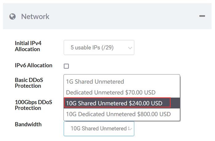
Sharktech10Gbps带宽,不限制流量,自带5个IPv4,100G防御
Sharktech荷兰10G带宽的独立服务器月付319美元起,10Gbps共享带宽,不限制流量,自带5个IPv4,免费60Gbps的 DDoS防御,可加到100G防御。CPU内存HDD价格购买地址E3-1270v216G2T$319/月链接E3-1270v516G2T$329/月链接2*E5-2670v232G2T$389/月链接2*E5-2678v364G2T$409/月链接这里我们需要注意,默...
日本美国站群服务器raksmart站群新增,限量低至月1.99美元
RAKsmart 商家八月份的促销活动今天更新。基本上和上个月的产品套餐活动差不多的,不过也是有简单的微调。对于RAKsmart商家还是比较了解的,他们家产品虽然这两年增加多个机房,以及在VPS主机方案上有丰富的机房和调整到一些自营机房,他们家的策划能力还是有限,基本上每个月的套餐活动都差不多。RAKsmart 在八月份看到有新增香港高防服务器可选,最高100GB防御。同时原来上个月缺货的日本独立...

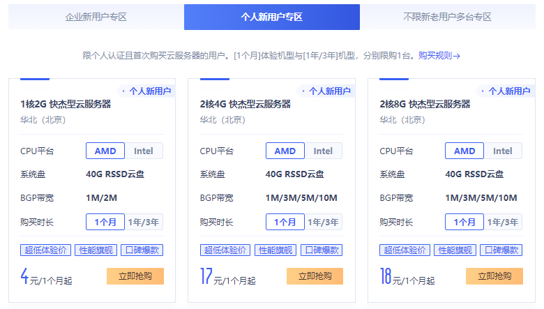
UCloud新人优惠中国香港/日本/美国云服务器低至4元
UCloud优刻得商家这几年应该已经被我们不少的个人站长用户认知,且确实在当下阿里云、腾讯云服务商不断的只促销服务于新用户活动,给我们很多老用户折扣的空间不多。于是,我们可以通过拓展选择其他同类服务商享受新人的福利,这里其中之一就选择UCloud商家。UCloud服务商2020年创业板上市的,实际上很早就有认识到,那时候价格高的离谱,谁让他们只服务有钱的企业用户呢。这里希望融入到我们大众消费者,你...
5xoy.com为你推荐
-
在线教育平台我想在网上教学,哪个网上教学平台好?站酷zcool谁能介绍几个矢量图的网站?巨星prince去世有几位好莱坞巨星死在2016年75ff.com开机出现www.ami.com是什么?怎么解决啊www.119mm.com看电影上什么网站??mole.61.com谁知道摩尔庄园的网址啊bbs2.99nets.com天堂1单机版到底怎么做www.ijinshan.com桌面上多了一个IE图标,打开后就链接到009dh.com这个网站,这个图标怎么删掉啊?dadi.tv智能网络电视smartTV是什么牌子www.175qq.com最炫的qq分组