Ciss华为p40pro限量套装
华为p40pro限量套装 时间:2021-05-03 阅读:()
SemiconductorComponentsIndustries,LLC,2017June,2019Rev.
21PublicationOrderNumber:FDMS8350LET40/DFDMS8350LET40MOSFETN‐ChannelPOWERTRENCH)40V,300A,0.
85mWGeneralDescriptionThisN-ChannelMVMOSFETisproducedusingONSemiconductor'sadvancedPOWERTRENCHprocessthathasbeenespeciallytailoredtominimizetheonstateresistanceandyetmaintainsuperiorswitchingperformance.
FeaturesMaxRDS(on)=0.
85mWatVGS=10V,ID=47AMaxRDS(on)=1.
2mWatVGS=4.
5V,ID=38AAdvancedPackageandSiliconcombinationforLowrDS(on)andHighEfficiencyMSL1RobustPackageDesign100%UILTestedTheseDevicesarePbFreeandareRoHSCompliantApplicationsPrimaryDCDCMOSFETSecondarySynchronousRectifierLoadSwitchMAXIMUMRATINGS(TA=25°Cunlessotherwisenoted)SymbolParameterValueUnitVDSDraintoSourceVoltage40VVGSGatetoSourceVoltage±20VIDDrainCurrent:Continuous(TC=25°C)(Note5)ContinuousTC=100°C(Note5)Continuous,TA=25°C(Note1a)Pulsed(Note4)300212491464AEASSinglePulseAvalancheEnergy(Note3)1176mJPDPowerDissipation:TC=25°CTA=25°C(Note1a)1253.
33WTJ,TSTGOperatingandStorageJunctionTemperatureRange55to+175°CStressesexceedingthoselistedintheMaximumRatingstablemaydamagethedevice.
Ifanyoftheselimitsareexceeded,devicefunctionalityshouldnotbeassumed,damagemayoccurandreliabilitymaybeaffected.
www.
onsemi.
comPQFN85X6,1.
27PCASE483AGSeedetailedorderingandshippinginformationonpage3ofthisdatasheet.
ORDERINGINFORMATIONN-CHANNELMOSFETMARKINGDIAGRAM$Y=ONSemiconductorLogo&Z=AssemblyPlantCode&3=DataCode(Year&Week)&K=LotFDMS8350LET40=SpecificDeviceCodeVDSRDS(ON)MAXIDMAX40V0.
85mW@10V47A1.
2mW@4.
5V$Y&Z&3&KFDMS8350LETDDDDSSSGBottomTopPin1GSSSDDDDSDGPin1FDMS8350LET40www.
onsemi.
com2THERMALCHARACTERISTICSSymbolParameterValueUnitRqJCThermalResistance,JunctiontoCase1.
2°C/WRqJAThermalResistance,JunctiontoAmbient(Note1a)45ELECTRICALCHARACTERISTICS(TJ=25°Cunlessotherwisenoted)SymbolParameterTestConditionMinTypMaxUnitOFFCHARACTERISTICSBVDSSDraintoSourceBreakdownVoltageID=250mA,VGS=0V40VDBVDSS/DTJBreakdownVoltageTemperatureCoefficientID=250mA,referencedto25°C17mV/°CIDSSZeroGateVoltageDrainCurrentVDS=32V,VGS=0V1mAIGSSGatetoSourceLeakageCurrentVGS=±20V,VDS=0V±100nAONCHARACTERISTICSVGS(th)GatetoSourceThresholdVoltageVGS=VDS,ID=250mA1.
01.
83.
0VDVGS(th)/DTJGatetoSourceThresholdVoltageTemperatureCoefficientID=250mA,referencedto25°C6mV/°CrDS(on)StaticDraintoSourceOnResistanceVGS=10V,ID=47A0.
680.
85mWVGS=4.
5V,ID=38A0.
961.
2VGS=10V,ID=47A,TJ=150°C1.
11.
4gFSForwardTransconductanceVDS=5V,ID=47A247SDYNAMICCHARACTERISTICSCissInputCapacitanceVDS=20V,VGS=0V,f=1MHz1185016590pFCossOutputCapacitance34304805pFCrssReverseTransferCapacitance69100pFRgGateResistance0.
11.
22.
4WSWITCHINGCHARACTERISTICStd(on)Turn-OnDelayTimeVDD=20V,ID=47A,VGS=10V,RGEN=6W3251nstrRiseTime1934nstd(off)Turn-OffDelayTime74118nstfFallTime1527nsQgTotalGateChargeVGS=0Vto10V156219nCVGS=0Vto4.
5V73102nCQgsGatetoSourceChargeVDD=20V,ID=47A33nCQgdGatetoDrain"Miller"ChargeVDD=20V,ID=47A16nCFDMS8350LET40www.
onsemi.
com3ELECTRICALCHARACTERISTICS(TJ=25°Cunlessotherwisenoted)(continued)SymbolUnitMaxTypMinTestConditionParameterDRAIN-SOURCEDIODECHARACTERISTICSVSDSourcetoDrainDiodeForwardVoltageVGS=0V,IS=2.
1A(Note2)0.
71.
2VVGS=0V,IS=47A(Note2)0.
81.
3trrReverseRecoveryTimeIF=47A,di/dt=100A/ms81129nsQrrReverseRecoveryCharge82131nCProductparametricperformanceisindicatedintheElectricalCharacteristicsforthelistedtestconditions,unlessotherwisenoted.
ProductperformancemaynotbeindicatedbytheElectricalCharacteristicsifoperatedunderdifferentconditions.
1.
RqJAisdeterminedwiththedevicemountedona1in2pad2ozcopperpadona1.
5*1.
5in.
boardofFR4material.
RqJCisguaranteedbydesignwhileRqCAisdeterminedbytheuser'sboarddesign.
NOTES:45°C/Wwhenmountedona1in2padof2ozcopper.
115°C/Wwhenmountedonaminimumpadof2ozcopper.
a)b)GDFDSSFSSGDFDSSFSS2.
PulseTest:PulseWidth<300ms,Dutycycle<2.
0%.
3.
EASof1176mJisbasedonstartingTJ=25°C;L=3mH,IAS=28A,VDD=40V,VGS=10V.
100%testatL=0.
1mH,IAS=87A.
4.
PulsedIdpleaserefertoFig11SOAgraphformoredetails.
5.
ComputedcontinuouscurrentlimitedtoMaxJunctionTemperatureonly,actualcontinuouscurrentwillbelimitedbythermal&electromechanicalapplicationboarddesign.
ORDERINGINFORMATIONDeviceMarkingPackageReelSizeTapeWidthQuantityFDMS8350LET40FDMS8350LETPower5613″12mm3000unitsFDMS8350LET40www.
onsemi.
com4TYPICALCHARACTERISTICS(TJ=25°Cunlessotherwisenoted)Figure1.
OnRegionCharacteristicsFigure2.
NormalizedOnResistancevsJunctionTemperatureFigure3.
OnResistancevsGatetoSourceVoltageFigure4.
TransferCharacteristics0.
00.
51.
01.
52.
02.
53.
0080160240320VGS=4VVGS=3.
5VVGS=4.
5VPULSEDURATION=80msDUTYCYCLE=0.
5%MAXVGS=3VVGS=10VID,DRAINCURRENT(A)VDS,DRAINTOSOURCEVOLTAGE(V)03691215VGS=3.
5VPULSEDURATION=80msDUTYCYCLE=0.
5%MAXNORMALIZEDDRAINTOSOURCEONRESISTANCEVGS=4VVGS=4.
5VVGS=3VVGS=10V75502502550751001251501750.
70.
80.
91.
01.
11.
21.
31.
41.
51.
61.
71.
8ID=47AVGS=10VNORMALIZEDDRAINTOSOURCEONRESISTANCETJ,JUNCTIONTEMPERATURE(oC)024681005101520TJ=150oCID=47ATJ=25oCVGS,GATETOSOURCEVOLTAGE(V)rDS(on),DRAINTOSOURCEONRESISTANCE(mW)PULSEDURATION=80msDUTYCYCLE=0.
5%MAX012345080160240320TJ=175oCVDS=5VPULSEDURATION=80msDUTYCYCLE=0.
5%MAXTJ=55oCTJ=25oCID,DRAINCURRENT(A)VGS,GATETOSOURCEVOLTAGE(V)TJ=55oCTJ=25oCTJ=175oCVGS=0VIS,REVERSEDRAINCURRENT(A)VSD,BODYDIODEFORWARDVOLTAGE(V)Figure5.
SourcetoDrainDiodeForwardVoltagevsSourceCurrent0.
00.
20.
40.
60.
81.
01.
20.
0010.
010.
1110100320Figure6.
NormalizedOnResistancevsDrainCurrentandGateVoltageI,DRAINCURRENT(A)D080160240320FDMS8350LET40www.
onsemi.
com5TYPICALCHARACTERISTICS(TJ=25°Cunlessotherwisenoted)Figure7.
GateChargeCharacteristicsFigure8.
CapacitancevsDraintoSourceVoltageFigure9.
UnclampedInductiveSwitchingCapabilityFigure10.
MaximumContinuousDrainCurrentvsCaseTemperatureFigure11.
ForwardBiasSafeOperatingAreaFigure12.
SinglePulseMaximumPowerDissipation034681021361700246810ID=47AVDD=25VVDD=20VVGS,GATETOSOURCEVOLTAGE(V)Qg,GATECHARGE(nC)VDD=15V0.
11104010100100000f=1MHzVGS=0VVDS,DRAINTOSOURCEVOLTAGE(V)CrssCossCiss0.
0010.
010.
1110100100010000110100200TJ=125oCTJ=25oCTJ=150oCtAV,TIMEINAVALANCHE(ms)IAS,AVALANCHECURRENT(A)255075100125150175080160240320VGS=4.
5VRqJC=1.
2oC/WVGS=10VID,DRAINCURRENT(A)TC,CASETEMPERATURE(oC)0.
010.
11101005000.
11101001000600010msCURVEBENTTOMEASUREDDATA100ms10ms100ms/DC1msID,DRAINCURRENT(A)VDS,DRAINtoSOURCEVOLTAGE(V)THISAREAISLIMITEDBYrDS(on)SINGLEPULSETJ=MAXRATEDRqJC=1.
2oC/WTC=25oC1051041031021011100100010000SINGLEPULSERqJC=1.
2oC/WTC=25oCP(PK),t,PULSEWIDTH(sec)50000PEAKTRANSIENTPOWER(W)CAPACITANCE(pF)100001000FDMS8350LET40www.
onsemi.
com6105104103102101112SINGLEPULSEDUTYCYCLEDESCENDINGORDERt,RECTANGULARPULSEDURATION(sec)D=0.
50.
20.
10.
050.
020.
01PDMt1t2NOTES:ZqJC(t)=r(t)xRqJCRqJC=1.
2oC/WDutyCycle,D=t1/t2PeakTJ=PDMxZqJC(t)+TCFigure13.
JunctiontoCaseTransientThermalResponseCurveTYPICALCHARACTERISTICS(TJ=25°Cunlessotherwisenoted)r(t),NORMALIZEDEFFECTIVETRANSIENTTHERMALRESISTANCE0.
0010.
010.
1PQFN85X6,1.
27PCASE483AGISSUEODATE30SEP2016MECHANICALCASEOUTLINEPACKAGEDIMENSIONSONSemiconductorandaretrademarksofSemiconductorComponentsIndustries,LLCdbaONSemiconductororitssubsidiariesintheUnitedStatesand/orothercountries.
ONSemiconductorreservestherighttomakechangeswithoutfurthernoticetoanyproductsherein.
ONSemiconductormakesnowarranty,representationorguaranteeregardingthesuitabilityofitsproductsforanyparticularpurpose,nordoesONSemiconductorassumeanyliabilityarisingoutoftheapplicationoruseofanyproductorcircuit,andspecificallydisclaimsanyandallliability,includingwithoutlimitationspecial,consequentialorincidentaldamages.
ONSemiconductordoesnotconveyanylicenseunderitspatentrightsnortherightsofothers.
98AON13657GDOCUMENTNUMBER:DESCRIPTION:ElectronicversionsareuncontrolledexceptwhenaccesseddirectlyfromtheDocumentRepository.
Printedversionsareuncontrolledexceptwhenstamped"CONTROLLEDCOPY"inred.
PAGE1OF1PQFN85X6,1.
27PSemiconductorComponentsIndustries,LLC,2019www.
onsemi.
comwww.
onsemi.
com1ONSemiconductorandaretrademarksofSemiconductorComponentsIndustries,LLCdbaONSemiconductororitssubsidiariesintheUnitedStatesand/orothercountries.
ONSemiconductorownstherightstoanumberofpatents,trademarks,copyrights,tradesecrets,andotherintellectualproperty.
AlistingofONSemiconductor'sproduct/patentcoveragemaybeaccessedatwww.
onsemi.
com/site/pdf/PatentMarking.
pdf.
ONSemiconductorreservestherighttomakechangeswithoutfurthernoticetoanyproductsherein.
ONSemiconductormakesnowarranty,representationorguaranteeregardingthesuitabilityofitsproductsforanyparticularpurpose,nordoesONSemiconductorassumeanyliabilityarisingoutoftheapplicationoruseofanyproductorcircuit,andspecificallydisclaimsanyandallliability,includingwithoutlimitationspecial,consequentialorincidentaldamages.
BuyerisresponsibleforitsproductsandapplicationsusingONSemiconductorproducts,includingcompliancewithalllaws,regulationsandsafetyrequirementsorstandards,regardlessofanysupportorapplicationsinformationprovidedbyONSemiconductor.
"Typical"parameterswhichmaybeprovidedinONSemiconductordatasheetsand/orspecificationscananddovaryindifferentapplicationsandactualperformancemayvaryovertime.
Alloperatingparameters,including"Typicals"mustbevalidatedforeachcustomerapplicationbycustomer'stechnicalexperts.
ONSemiconductordoesnotconveyanylicenseunderitspatentrightsnortherightsofothers.
ONSemiconductorproductsarenotdesigned,intended,orauthorizedforuseasacriticalcomponentinlifesupportsystemsoranyFDAClass3medicaldevicesormedicaldeviceswithasameorsimilarclassificationinaforeignjurisdictionoranydevicesintendedforimplantationinthehumanbody.
ShouldBuyerpurchaseoruseONSemiconductorproductsforanysuchunintendedorunauthorizedapplication,BuyershallindemnifyandholdONSemiconductoranditsofficers,employees,subsidiaries,affiliates,anddistributorsharmlessagainstallclaims,costs,damages,andexpenses,andreasonableattorneyfeesarisingoutof,directlyorindirectly,anyclaimofpersonalinjuryordeathassociatedwithsuchunintendedorunauthorizeduse,evenifsuchclaimallegesthatONSemiconductorwasnegligentregardingthedesignormanufactureofthepart.
ONSemiconductorisanEqualOpportunity/AffirmativeActionEmployer.
Thisliteratureissubjecttoallapplicablecopyrightlawsandisnotforresaleinanymanner.
PUBLICATIONORDERINGINFORMATIONTECHNICALSUPPORTNorthAmericanTechnicalSupport:VoiceMail:18002829855TollFreeUSA/CanadaPhone:011421337902910LITERATUREFULFILLMENT:EmailRequeststo:orderlit@onsemi.
comONSemiconductorWebsite:www.
onsemi.
comEurope,MiddleEastandAfricaTechnicalSupport:Phone:00421337902910Foradditionalinformation,pleasecontactyourlocalSalesRepresentative
- Ciss华为p40pro限量套装相关文档
- 谨请参阅尾页重要声明及华泰证券股票和行业评级标准
- TL(RE,RME,SE,OE,YE)16TP(F)
- 河南省第三强制隔离戒毒所智慧戒毒管控管理系统
- grinding华为p40pro限量套装
- response华为p40pro限量套装
- 三星华为p40pro限量套装
物语云-VPS-美国洛杉矶VPS无限流量云windows大带宽100M不限流量 26/月起
物语云计算怎么样?物语云计算(MonogatariCloud)是一家成立于2016年的老牌国人商家,主营国内游戏高防独服业务,拥有多家机房资源,产品质量过硬,颇有一定口碑。本次带来的是特惠活动为美国洛杉矶Cera机房的不限流量大带宽VPS,去程直连回程4837,支持免费安装Windows系统。值得注意的是,物语云采用的虚拟化技术为Hyper-v,因此并不会超售超开。一、物语云官网点击此处进入物语云...

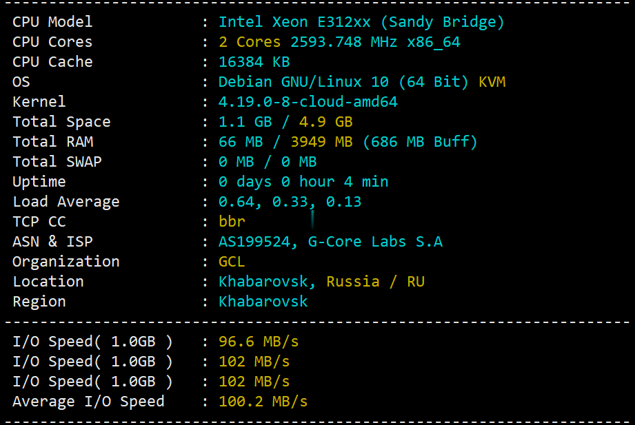
gcorelabs远东khabarovsk伯力Cloud云服务器测评,告诉你gcorelabs云服务器怎么样
说明一下:gcorelabs的俄罗斯远东机房“伯力”既有“Virtual servers”也有“CLOUD SERVICES”,前者是VPS,后者是云服务器,不是一回事;由于平日大家习惯把VPS和云服务器当做一回事儿,所以这里要特别说明一下。本次测评的是gcorelabs的cloud,也就是云服务器。 官方网站:https://gcorelabs.com 支持:数字加密货币、信用卡、PayPal...
10gbiz首月半价月付2.36美元,香港/洛杉矶VPS、硅谷独立服务器/站群服务器
收到10gbiz发来的7月份优惠方案,中国香港、美国洛杉矶机房VPS主机4折优惠码,优惠后洛杉矶VPS月付2.36美元起,香港VPS月付2.75美元起。这是一家2020年成立的主机商,提供的产品包括独立服务器租用和VPS主机等,数据中心在美国洛杉矶、圣何塞和中国香港。商家VPS主机基于KVM架构,支持使用PayPal或者支付宝付款。洛杉矶VPS架构CPU内存硬盘带宽系统价格单核512MB10GB1...

华为p40pro限量套装为你推荐
-
signal37新iphone也将禁售iPhone8plus在2020年还会有货吗课程cuteftp加多宝和王老吉王老吉和加多宝是什么关系刚刚网女友刚开始用震动棒很舒服身上抽搐时,她说疼不让用了,是真的疼还是太刺激她受不了?什么是seoSEO网站优化是什么啊?开源网店开源网店系统 独立网店系统 淘宝 有什么区别?qq挂件如何使QQ气泡和挂件成为永久的?图文模块为什么我的QQ弄了图文模块只出现字没有图片?图文模块图文模块的标题栏填什么啊?