shift7xxuu.com
7xxuu.com 时间:2021-04-08 阅读:()
DS180(v2.
6.
1)September8,2020www.
xilinx.
comProductSpecification1Copyright2010–2020Xilinx,Inc.
Xilinx,theXilinxlogo,Alveo,Artix,Kintex,Spartan,UltraScale,Versal,Virtex,Vivado,Zynq,andotherdesignatedbrandsincludedhereinaretrademarksofXilinxintheUnitedStatesandothercountries.
PCI,PCIExpress,PCIe,andPCI-XaretrademarksofPCI-SIG.
Allothertrademarksarethepropertyoftheirrespectiveowners.
GeneralDescriptionXilinx7seriesFPGAscomprisefourFPGAfamiliesthataddressthecompleterangeofsystemrequirements,rangingfromlowcost,smallformfactor,cost-sensitive,high-volumeapplicationstoultrahigh-endconnectivitybandwidth,logiccapacity,andsignalprocessingcapabilityforthemostdemandinghigh-performanceapplications.
The7seriesFPGAsinclude:Spartan-7Family:Optimizedforlowcost,lowestpower,andhighI/Operformance.
Availableinlow-cost,verysmallform-factorpackagingforsmallestPCBfootprint.
Artix-7Family:OptimizedforlowpowerapplicationsrequiringserialtransceiversandhighDSPandlogicthroughput.
Providesthelowesttotalbillofmaterialscostforhigh-throughput,cost-sensitiveapplications.
Kintex-7Family:Optimizedforbestprice-performancewitha2Ximprovementcomparedtopreviousgeneration,enablinganewclassofFPGAs.
Virtex-7Family:Optimizedforhighestsystemperformanceandcapacitywitha2Ximprovementinsystemperformance.
Highestcapabilitydevicesenabledbystackedsiliconinterconnect(SSI)technology.
Builtonastate-of-the-art,high-performance,low-power(HPL),28nm,high-kmetalgate(HKMG)processtechnology,7seriesFPGAsenableanunparalleledincreaseinsystemperformancewith2.
9Tb/sofI/Obandwidth,2millionlogiccellcapacity,and5.
3TMAC/sDSP,whileconsuming50%lesspowerthanpreviousgenerationdevicestoofferafullyprogrammablealternativetoASSPsandASICs.
Summaryof7SeriesFPGAFeaturesAdvancedhigh-performanceFPGAlogicbasedonreal6-inputlook-uptable(LUT)technologyconfigurableasdistributedmemory.
36Kbdual-portblockRAMwithbuilt-inFIFOlogicforon-chipdatabuffering.
High-performanceSelectIOtechnologywithsupportforDDR3interfacesupto1,866Mb/s.
High-speedserialconnectivitywithbuilt-inmulti-gigabittransceiversfrom600Mb/stomax.
ratesof6.
6Gb/supto28.
05Gb/s,offeringaspeciallow-powermode,optimizedforchip-to-chipinterfaces.
Auserconfigurableanaloginterface(XADC),incorporatingdual12-bit1MSPSanalog-to-digitalconverterswithon-chipthermalandsupplysensors.
DSPsliceswith25x18multiplier,48-bitaccumulator,andpre-adderforhigh-performancefiltering,includingoptimizedsymmetriccoefficientfiltering.
Powerfulclockmanagementtiles(CMT),combiningphase-lockedloop(PLL)andmixed-modeclockmanager(MMCM)blocksforhighprecisionandlowjitter.
QuicklydeployembeddedprocessingwithMicroBlazeprocessor.
IntegratedblockforPCIExpress(PCIe),foruptox8Gen3EndpointandRootPortdesigns.
Widevarietyofconfigurationoptions,includingsupportforcommoditymemories,256-bitAESencryptionwithHMAC/SHA-256authentication,andbuilt-inSEUdetectionandcorrection.
Low-cost,wire-bond,bare-dieflip-chip,andhighsignalintegrityflip-chippackagingofferingeasymigrationbetweenfamilymembersinthesamepackage.
AllpackagesavailableinPb-freeandselectedpackagesinPboption.
Designedforhighperformanceandlowestpowerwith28nm,HKMG,HPLprocess,1.
0Vcorevoltageprocesstechnologyand0.
9Vcorevoltageoptionforevenlowerpower.
197SeriesFPGAsDataSheet:OverviewDS180(v2.
6.
1)September8,2020ProductSpecificationTable1:7SeriesFamiliesComparisonMax.
CapabilitySpartan-7Artix-7Kintex-7Virtex-7LogicCells102K215K478K1,955KBlockRAM(1)4.
2Mb13Mb34Mb68MbDSPSlices1607401,9203,600DSPPerformance(2)176GMAC/s929GMAC/s2,845GMAC/s5,335GMAC/sMicroBlazeCPU(3)260DMIPs303DMIPs438DMIPs441DMIPsTransceivers–163296TransceiverSpeed–6.
6Gb/s12.
5Gb/s28.
05Gb/sSerialBandwidth–211Gb/s800Gb/s2,784Gb/sPCIeInterface–x4Gen2x8Gen2x8Gen3MemoryInterface800Mb/s1,066Mb/s1,866Mb/s1,866Mb/sI/OPins4005005001,200I/OVoltage1.
2V–3.
3V1.
2V–3.
3V1.
2V–3.
3V1.
2V–3.
3VPackageOptionsLow-Cost,Wire-BondLow-Cost,Wire-Bond,Bare-DieFlip-ChipBare-DieFlip-ChipandHigh-PerformanceFlip-ChipHighestPerformanceFlip-ChipNotes:1.
AdditionalmemoryavailableintheformofdistributedRAM.
2.
PeakDSPperformancenumbersarebasedonsymmetricalfilterimplementation.
3.
PeakMicroBlazeCPUperformancenumbersbasedonmicrocontrollerpreset.
7SeriesFPGAsDataSheet:OverviewDS180(v2.
6.
1)September8,2020www.
xilinx.
comProductSpecification2Spartan-7FPGAFeatureSummaryTable2:Spartan-7FPGAFeatureSummarybyDeviceDeviceLogicCellsCLBDSPSlices(2)BlockRAMBlocks(3)CMTs(4)PCIeGTXADCBlocksTotalI/OBanks(5)MaxUserI/OSlices(1)MaxDistributedRAM(Kb)18Kb36KbMax(Kb)XC7S66,000938701010518020002100XC7S1512,8002,00015020201036020002100XC7S2523,3603,6503138090451,62030013150XC7S5052,1608,150600120150752,70050015250XC7S7576,80012,000832140180903,24080018400XC7S100102,40016,0001,1001602401204,32080018400Notes:1.
Each7seriesFPGAslicecontainsfourLUTsandeightflip-flops;onlysomeslicescanusetheirLUTsasdistributedRAMorSRLs.
2.
EachDSPslicecontainsapre-adder,a25x18multiplier,anadder,andanaccumulator.
3.
BlockRAMsarefundamentally36Kbinsize;eachblockcanalsobeusedastwoindependent18Kbblocks.
4.
EachCMTcontainsoneMMCMandonePLL.
5.
DoesnotincludeconfigurationBank0.
Table3:Spartan-7FPGADevice-PackageCombinationsandMaximumI/OsPackageCPGA196CSGA225CSGA324FTGB196FGGA484FGGA676Size(mm)8x813x1315x1515x1523x2327x27BallPitch(mm)0.
50.
80.
81.
01.
01.
0DeviceHRI/O(1)HRI/O(1)HRI/O(1)HRI/O(1)HRI/O(1)HRI/O(1)XC7S6100100100XC7S15100100100XC7S25150150100XC7S50210100250XC7S75338400XC7S100338400Notes:1.
HR=High-rangeI/OwithsupportforI/Ovoltagefrom1.
2Vto3.
3V.
7SeriesFPGAsDataSheet:OverviewDS180(v2.
6.
1)September8,2020www.
xilinx.
comProductSpecification3Artix-7FPGAFeatureSummaryTable4:Artix-7FPGAFeatureSummarybyDeviceDeviceLogicCellsConfigurableLogicBlocks(CLBs)DSP48E1Slices(2)BlockRAMBlocks(3)CMTs(4)PCIe(5)GTPsXADCBlocksTotalI/OBanks(6)MaxUserI/O(7)Slices(1)MaxDistributedRAM(Kb)18Kb36KbMax(Kb)XC7A12T12,8002,00017140402072031213150XC7A15T16,6402,60020045502590051415250XC7A25T23,3603,6503138090451,62031413150XC7A35T33,2805,20040090100501,80051415250XC7A50T52,1608,150600120150752,70051415250XC7A75T75,52011,8008921802101053,78061816300XC7A100T101,44015,8501,1882402701354,86061816300XC7A200T215,36033,6502,88874073036513,14010116110500Notes:1.
Each7seriesFPGAslicecontainsfourLUTsandeightflip-flops;onlysomeslicescanusetheirLUTsasdistributedRAMorSRLs.
2.
EachDSPslicecontainsapre-adder,a25x18multiplier,anadder,andanaccumulator.
3.
BlockRAMsarefundamentally36Kbinsize;eachblockcanalsobeusedastwoindependent18Kbblocks.
4.
EachCMTcontainsoneMMCMandonePLL.
5.
Artix-7FPGAInterfaceBlocksforPCIExpresssupportuptox4Gen2.
6.
DoesnotincludeconfigurationBank0.
7.
ThisnumberdoesnotincludeGTPtransceivers.
Table5:Artix-7FPGADevice-PackageCombinationsandMaximumI/OsPackage(1)CPG236CPG238CSG324CSG325FTG256SBG484FGG484(2)FBG484(2)FGG676(3)FBG676(3)FFG1156Size(mm)10x1010x1015x1515x1517x1719x1923x2323x2327x2727x2735x35BallPitch(mm)0.
50.
50.
80.
81.
00.
81.
01.
01.
01.
01.
0DeviceGTP(4)I/OGTP(4)I/OGTP(4)I/OGTP(4)I/OGTP(4)I/OGTPI/OGTP(4)I/OGTPI/OGTP(4)I/OGTPI/OGTPI/OHR(5)HR(5)HR(5)HR(5)HR(5)HR(5)HR(5)HR(5)HR(5)HR(5)HR(5)XC7A12T21122150XC7A15T21060210415001704250XC7A25T21124150XC7A35T21060210415001704250XC7A50T21060210415001704250XC7A75T0210017042858300XC7A100T0210017042858300XC7A200T42854285840016500Notes:1.
AllpackageslistedarePb-free(SBG,FBG,FFGwithexemption15).
SomepackagesareavailableinPboption.
2.
DevicesinFGG484andFBG484arefootprintcompatible.
3.
DevicesinFGG676andFBG676arefootprintcompatible.
4.
GTPtransceiversinCP,CS,FT,andFGpackagessupportdataratesupto6.
25Gb/s.
5.
HR=High-rangeI/OwithsupportforI/Ovoltagefrom1.
2Vto3.
3V.
7SeriesFPGAsDataSheet:OverviewDS180(v2.
6.
1)September8,2020www.
xilinx.
comProductSpecification4Kintex-7FPGAFeatureSummaryTable6:Kintex-7FPGAFeatureSummarybyDeviceDeviceLogicCellsConfigurableLogicBlocks(CLBs)DSPSlices(2)BlockRAMBlocks(3)CMTs(4)PCIe(5)GTXsXADCBlocksTotalI/OBanks(6)MaxUserI/O(7)Slices(1)MaxDistributedRAM(Kb)18Kb36KbMax(Kb)XC7K70T65,60010,2508382402701354,86061816300XC7K160T162,24025,3502,18860065032511,70081818400XC7K325T326,08050,9504,00084089044516,02010116110500XC7K355T356,16055,6505,0881,4401,43071525,740612416300XC7K410T406,72063,5505,6631,5401,59079528,62010116110500XC7K420T416,96065,1505,9381,6801,67083530,060813218400XC7K480T477,76074,6506,7881,9201,91095534,380813218400Notes:1.
Each7seriesFPGAslicecontainsfourLUTsandeightflip-flops;onlysomeslicescanusetheirLUTsasdistributedRAMorSRLs.
2.
EachDSPslicecontainsapre-adder,a25x18multiplier,anadder,andanaccumulator.
3.
BlockRAMsarefundamentally36Kbinsize;eachblockcanalsobeusedastwoindependent18Kbblocks.
4.
EachCMTcontainsoneMMCMandonePLL.
5.
Kintex-7FPGAInterfaceBlocksforPCIExpresssupportuptox8Gen2.
6.
DoesnotincludeconfigurationBank0.
7.
ThisnumberdoesnotincludeGTXtransceivers.
Table7:Kintex-7FPGADevice-PackageCombinationsandMaximumI/OsPackage(1)FBG484FBG676(2)FFG676(2)FBG900(3)FFG900(3)FFG901FFG1156Size(mm)23x2327x2727x2731x3131x3131x3135x35BallPitch(mm)1.
01.
01.
01.
01.
01.
01.
0DeviceGTX(4)I/OGTX(4)I/OGTXI/OGTX(4)I/OGTXI/OGTXI/OGTXI/OHR(5)HP(6)HR(5)HP(6)HR(5)HP(6)HR(5)HP(6)HR(5)HP(6)HR(5)HP(6)HR(5)HP(6)XC7K70T41851008200100XC7K160T418510082501508250150XC7K325T825015082501501635015016350150XC7K355T243000XC7K410T825015082501501635015016350150XC7K420T283800324000XC7K480T283800324000Notes:1.
AllpackageslistedarePb-free(FBG,FFGwithexemption15).
SomepackagesareavailableinPboption.
2.
DevicesinFBG676andFFG676arefootprintcompatible.
3.
DevicesinFBG900andFFG900arefootprintcompatible.
4.
GTXtransceiversinFBpackagessupportthefollowingmaximumdatarates:10.
3Gb/sinFBG484;6.
6Gb/sinFBG676andFBG900.
RefertoKintex-7FPGAsDataSheet:DCandACSwitchingCharacteristics(DS182)fordetails.
5.
HR=High-rangeI/OwithsupportforI/Ovoltagefrom1.
2Vto3.
3V.
6.
HP=High-performanceI/OwithsupportforI/Ovoltagefrom1.
2Vto1.
8V.
7SeriesFPGAsDataSheet:OverviewDS180(v2.
6.
1)September8,2020www.
xilinx.
comProductSpecification5Virtex-7FPGAFeatureSummaryTable8:Virtex-7FPGAFeatureSummaryDeviceLogicCellsConfigurableLogicBlocks(CLBs)DSPSlices(2)BlockRAMBlocks(3)CMTs(4)PCIe(5)GTXGTHGTZXADCBlocksTotalI/OBanks(6)MaxUserI/O(7)SLRs(8)Slices(1)MaxDistributedRAM(Kb)18Kb36KbMax(Kb)XC7V585T582,72091,0506,9381,2601,59079528,6201833600117850N/AXC7V2000T1,954,560305,40021,5502,1602,5841,29246,51224436001241,2004XC7VX330T326,40051,0004,3881,1201,50075027,0001420280114700N/AXC7VX415T412,16064,4006,5252,1601,76088031,6801220480112600N/AXC7VX485T485,76075,9008,1752,8002,0601,03037,0801445600114700N/AXC7VX550T554,24086,6008,7252,8802,3601,18042,4802020800116600N/AXC7VX690T693,120108,30010,8883,6002,9401,47052,92020308001201,000N/AXC7VX980T979,200153,00013,8383,6003,0001,50054,0001830720118900N/AXC7VX1140T1,139,200178,00017,7003,3603,7601,88067,68024409601221,1004XC7VH580T580,48090,7008,8501,6801,88094033,84012204881126002XC7VH870T876,160136,90013,2752,5202,8201,41050,76018307216163003Notes:1.
Each7seriesFPGAslicecontainsfourLUTsandeightflip-flops;onlysomeslicescanusetheirLUTsasdistributedRAMorSRLs.
2.
EachDSPslicecontainsapre-adder,a25x18multiplier,anadder,andanaccumulator.
3.
BlockRAMsarefundamentally36Kbinsize;eachblockcanalsobeusedastwoindependent18Kbblocks.
4.
EachCMTcontainsoneMMCMandonePLL.
5.
Virtex-7TFPGAInterfaceBlocksforPCIExpresssupportuptox8Gen2.
Virtex-7XTandVirtex-7HTInterfaceBlocksforPCIExpresssupportuptox8Gen3,withtheexceptionoftheXC7VX485Tdevice,whichsupportsx8Gen2.
6.
DoesnotincludeconfigurationBank0.
7.
ThisnumberdoesnotincludeGTX,GTH,orGTZtransceivers.
8.
Superlogicregions(SLRs)aretheconstituentpartsofFPGAsthatuseSSItechnology.
Virtex-7HTdevicesuseSSItechnologytoconnectSLRswith28.
05Gb/stransceivers.
7SeriesFPGAsDataSheet:OverviewDS180(v2.
6.
1)September8,2020www.
xilinx.
comProductSpecification6Table9:Virtex-7FPGADevice-PackageCombinationsandMaximumI/OsPackage(1)FFG1157FFG1761(2)FHG1761(2)FLG1925Size(mm)35x3542.
5x42.
545x4545x45BallPitch1.
01.
01.
01.
0DeviceGTXGTHI/OGTXGTHI/OGTXGTHI/OGTXI/OHR(3)HP(4)HR(3)HP(4)HR(3)HP(4)HR(3)HP(4)XC7V585T2000600360100750XC7V2000T36008501601,200XC7VX330T020060002850650XC7VX415T0200600XC7VX485T20006002800700XC7VX550TXC7VX690T02006000360850XC7VX980TXC7VX1140TNotes:1.
AllpackageslistedarePb-free(FFG,FHG,FLGwithexemption15).
SomepackagesareavailableinPboption.
2.
DevicesinFFG1761andFHG1761arefootprintcompatible.
3.
HR=High-rangeI/OwithsupportforI/Ovoltagefrom1.
2Vto3.
3V.
4.
HP=High-performanceI/OwithsupportforI/Ovoltagefrom1.
2Vto1.
8V.
Table10:Virtex-7FPGADevice-PackageCombinationsandMaximumI/Os-ContinuedPackage(1)FFG1158FFG1926(2)FLG1926(2)FFG1927FFG1928(3)FLG1928(3)FFG1930(4)FLG1930(4)Size(mm)35x3545x4545x4545x4545x4545x4545x4545x45BallPitch1.
01.
01.
01.
01.
01.
01.
01.
0DeviceGTXGTHI/OGTXGTHI/OGTXGTHI/OGTXGTHI/OGTXGTHI/OGTXGTHI/OGTXGTHI/OGTXGTHI/OHP(5)HP(5)HP(5)HP(5)HP(5)HP(5)HP(5)HP(5)XC7V585TXC7V2000TXC7VX330TXC7VX415T048350048600XC7VX485T480350560600240700XC7VX550T048350080600XC7VX690T0483500647200806000241,000XC7VX980T064720072480024900XC7VX1140T0647200964800241,100Notes:1.
AllpackageslistedarePb-free(FFG,FLGwithexemption15).
SomepackagesareavailableinPboption.
2.
DevicesinFFG1926andFLG1926arefootprintcompatible.
3.
DevicesinFFG1928andFLG1928arefootprintcompatible.
4.
DevicesinFFG1930andFLG1930arefootprintcompatible.
5.
HP=High-performanceI/OwithsupportforI/Ovoltagefrom1.
2Vto1.
8V.
7SeriesFPGAsDataSheet:OverviewDS180(v2.
6.
1)September8,2020www.
xilinx.
comProductSpecification7StackedSiliconInterconnect(SSI)TechnologyTherearemanychallengesassociatedwithcreatinghighcapacityFPGAsthatXilinxaddresseswiththeSSItechnology.
SSItechnologyenablesmultiplesuperlogicregions(SLRs)tobecombinedonapassiveinterposerlayer,usingprovenmanufacturingandassemblytechniquesfromindustryleaders,tocreateasingleFPGAwithmorethantenthousandinter-SLRconnections,providingultra-highbandwidthconnectivitywithlowlatencyandlowpowerconsumption.
TherearetwotypesofSLRsusedinVirtex-7FPGAs:alogicintensiveSLRusedintheVirtex-7TdevicesandaDSP/blockRAM/transceiver-richSLRusedintheVirtex-7XTandHTdevices.
SSItechnologyenablestheproductionofhighercapabilityFPGAsthantraditionalmanufacturingmethods,enablingthehighestcapacityandhighestperformanceFPGAsevercreatedtoreachproductionmorequicklyandwithlessriskthanwouldotherwisebepossible.
Thousandsofsuperlongline(SLL)routingresourcesandultra-highperformanceclocklinesthatcrossbetweentheSLRsensurethatdesignsspanseamlesslyacrossthesehigh-densityprogrammablelogicdevices.
CLBs,Slices,andLUTsSomekeyfeaturesoftheCLBarchitectureinclude:Real6-inputlook-uptables(LUTs)MemorycapabilitywithintheLUTRegisterandshiftregisterfunctionalityTheLUTsin7seriesFPGAscanbeconfiguredaseitherone6-inputLUT(64-bitROMs)withoneoutput,orastwo5-inputLUTs(32-bitROMs)withseparateoutputsbutcommonaddressesorlogicinputs.
EachLUToutputcanoptionallyberegisteredinaflip-flop.
FoursuchLUTsandtheireightflip-flopsaswellasmultiplexersandarithmeticcarrylogicformaslice,andtwoslicesformaconfigurablelogicblock(CLB).
Fouroftheeightflip-flopsperslice(oneperLUT)canoptionallybeconfiguredaslatches.
Between25–50%ofallslicescanalsousetheirLUTsasdistributed64-bitRAMoras32-bitshiftregisters(SRL32)orastwoSRL16s.
Modernsynthesistoolstakeadvantageofthesehighlyefficientlogic,arithmetic,andmemoryfeatures.
ClockManagementSomeofthekeyhighlightsoftheclockmanagementarchitectureinclude:High-speedbuffersandroutingforlow-skewclockdistributionFrequencysynthesisandphaseshiftingLow-jitterclockgenerationandjitterfilteringEach7seriesFPGAhasupto24clockmanagementtiles(CMTs),eachconsistingofonemixed-modeclockmanager(MMCM)andonephase-lockedloop(PLL).
Table11:Virtex-7HTFPGADevice-PackageCombinationsandMaximumI/OsPackage(1)FLG1155FLG1931FLG1932Size(mm)35x3545x4545x45BallPitch1.
01.
01.
0DeviceGTHGTZI/OGTHGTZI/OGTHGTZI/OHP(2)HP(2)HP(2)XC7VH580T248400488600XC7VH870T7216300Notes:1.
AllpackageslistedarePb-freewithexemption15.
SomepackagesareavailableinPboption.
2.
HP=High-performanceI/OwithsupportforI/Ovoltagefrom1.
2Vto1.
8V.
7SeriesFPGAsDataSheet:OverviewDS180(v2.
6.
1)September8,2020www.
xilinx.
comProductSpecification8Mixed-ModeClockManagerandPhase-LockedLoopTheMMCMandPLLsharemanycharacteristics.
Bothcanserveasafrequencysynthesizerforawiderangeoffrequenciesandasajitterfilterforincomingclocks.
Atthecenterofbothcomponentsisavoltage-controlledoscillator(VCO),whichspeedsupandslowsdowndependingontheinputvoltageitreceivesfromthephasefrequencydetector(PFD).
Therearethreesetsofprogrammablefrequencydividers:D,M,andO.
Thepre-dividerD(programmablebyconfigurationandafterwardsviaDRP)reducestheinputfrequencyandfeedsoneinputofthetraditionalPLLphase/frequencycomparator.
ThefeedbackdividerM(programmablebyconfigurationandafterwardsviaDRP)actsasamultiplierbecauseitdividestheVCOoutputfrequencybeforefeedingtheotherinputofthephasecomparator.
DandMmustbechosenappropriatelytokeeptheVCOwithinitsspecifiedfrequencyrange.
TheVCOhaseightequally-spacedoutputphases(0°,45°,90°,135°,180°,225°,270°,and315°).
Eachcanbeselectedtodriveoneoftheoutputdividers(sixforthePLL,O0toO5,andsevenfortheMMCM,O0toO6),eachprogrammablebyconfigurationtodividebyanyintegerfrom1to128.
TheMMCMandPLLhavethreeinput-jitterfilteroptions:lowbandwidth,highbandwidth,oroptimizedmode.
Low-bandwidthmodehasthebestjitterattenuationbutnotthesmallestphaseoffset.
High-bandwidthmodehasthebestphaseoffset,butnotthebestjitterattenuation.
Optimizedmodeallowsthetoolstofindthebestsetting.
MMCMAdditionalProgrammableFeaturesTheMMCMcanhaveafractionalcounterineitherthefeedbackpath(actingasamultiplier)orinoneoutputpath.
Fractionalcountersallownon-integerincrementsof1/8andcanthusincreasefrequencysynthesiscapabilitiesbyafactorof8.
TheMMCMcanalsoprovidefixedordynamicphaseshiftinsmallincrementsthatdependontheVCOfrequency.
At1600MHz,thephase-shifttimingincrementis11.
2ps.
ClockDistributionEach7seriesFPGAprovidessixdifferenttypesofclocklines(BUFG,BUFR,BUFIO,BUFH,BUFMR,andthehigh-performanceclock)toaddressthedifferentclockingrequirementsofhighfanout,shortpropagationdelay,andextremelylowskew.
GlobalClockLinesIneach7seriesFPGA(exceptXC7S6andXC7S15),32globalclocklineshavethehighestfanoutandcanreacheveryflip-flopclock,clockenable,andset/reset,aswellasmanylogicinputs.
Thereare12globalclocklineswithinanyclockregiondrivenbythehorizontalclockbuffers(BUFH).
EachBUFHcanbeindependentlyenabled/disabled,allowingforclockstobeturnedoffwithinaregion,therebyofferingfine-graincontroloverwhichclockregionsconsumepower.
Globalclocklinescanbedrivenbyglobalclockbuffers,whichcanalsoperformglitchlessclockmultiplexingandclockenablefunctions.
GlobalclocksareoftendrivenfromtheCMT,whichcancompletelyeliminatethebasicclockdistributiondelay.
RegionalClocksRegionalclockscandriveallclockdestinationsintheirregion.
Aregionisdefinedasanareathatis50I/Oand50CLBhighandhalfthechipwide.
7seriesFPGAshavebetweentwoandtwenty-fourregions.
Therearefourregionalclocktracksineveryregion.
Eachregionalclockbuffercanbedrivenfromanyoffourclock-capableinputpins,anditsfrequencycanoptionallybedividedbyanyintegerfrom1to8.
I/OClocksI/OclocksareespeciallyfastandserveonlyI/Ologicandserializer/deserializer(SerDes)circuits,asdescribedintheI/OLogicsection.
The7seriesdeviceshaveadirectconnectionfromtheMMCMtotheI/Oforlow-jitter,high-performanceinterfaces.
7SeriesFPGAsDataSheet:OverviewDS180(v2.
6.
1)September8,2020www.
xilinx.
comProductSpecification9BlockRAMSomeofthekeyfeaturesoftheblockRAMinclude:Dual-port36KbblockRAMwithportwidthsofupto72ProgrammableFIFOlogicBuilt-inoptionalerrorcorrectioncircuitryEvery7seriesFPGAhasbetween5and1,880dual-portblockRAMs,eachstoring36Kb.
EachblockRAMhastwocompletelyindependentportsthatsharenothingbutthestoreddata.
SynchronousOperationEachmemoryaccess,readorwrite,iscontrolledbytheclock.
Allinputs,data,address,clockenables,andwriteenablesareregistered.
Nothinghappenswithoutaclock.
Theinputaddressisalwaysclocked,retainingdatauntilthenextoperation.
Anoptionaloutputdatapipelineregisterallowshigherclockratesatthecostofanextracycleoflatency.
Duringawriteoperation,thedataoutputcanreflecteitherthepreviouslystoreddata,thenewlywrittendata,orcanremainunchanged.
ProgrammableDataWidthEachportcanbeconfiguredas32K*1,16K*2,8K*4,4K*9(or8),2K*18(or16),1K*36(or32),or512*72(or64).
Thetwoportscanhavedifferentaspectratioswithoutanyconstraints.
EachblockRAMcanbedividedintotwocompletelyindependent18KbblockRAMsthatcaneachbeconfiguredtoanyaspectratiofrom16K*1to512*36.
Everythingdescribedpreviouslyforthefull36KbblockRAMalsoappliestoeachofthesmaller18KbblockRAMs.
Onlyinsimpledual-port(SDP)modecandatawidthsofgreaterthan18bits(18KbRAM)or36bits(36KbRAM)beaccessed.
Inthismode,oneportisdedicatedtoreadoperation,theothertowriteoperation.
InSDPmode,oneside(readorwrite)canbevariable,whiletheotherisfixedto32/36or64/72.
Bothsidesofthedual-port36KbRAMcanbeofvariablewidth.
Twoadjacent36KbblockRAMscanbeconfiguredasonecascaded64K*1dual-portRAMwithoutanyadditionallogic.
ErrorDetectionandCorrectionEach64-bit-wideblockRAMcangenerate,store,andutilizeeightadditionalHammingcodebitsandperformsingle-biterrorcorrectionanddouble-biterrordetection(ECC)duringthereadprocess.
TheECClogiccanalsobeusedwhenwritingtoorreadingfromexternal64-to72-bit-widememories.
FIFOControllerThebuilt-inFIFOcontrollerforsingle-clock(synchronous)ordual-clock(asynchronousormultirate)operationincrementstheinternaladdressesandprovidesfourhandshakingflags:full,empty,almostfull,andalmostempty.
Thealmostfullandalmostemptyflagsarefreelyprogrammable.
SimilartotheblockRAM,theFIFOwidthanddepthareprogrammable,butthewriteandreadportsalwayshaveidenticalwidth.
Firstwordfall-throughmodepresentsthefirst-writtenwordonthedataoutputevenbeforethefirstreadoperation.
Afterthefirstwordhasbeenread,thereisnodifferencebetweenthismodeandthestandardmode.
7SeriesFPGAsDataSheet:OverviewDS180(v2.
6.
1)September8,2020www.
xilinx.
comProductSpecification10DigitalSignalProcessing—DSPSliceSomehighlightsoftheDSPfunctionalityinclude:25*18two'scomplementmultiplier/accumulatorhigh-resolution(48bit)signalprocessorPowersavingpre-addertooptimizesymmetricalfilterapplicationsAdvancedfeatures:optionalpipelining,optionalALU,anddedicatedbusesforcascadingDSPapplicationsusemanybinarymultipliersandaccumulators,bestimplementedindedicatedDSPslices.
All7seriesFPGAshavemanydedicated,fullcustom,low-powerDSPslices,combininghighspeedwithsmallsizewhileretainingsystemdesignflexibility.
EachDSPslicefundamentallyconsistsofadedicated25*18bittwo'scomplementmultiplieranda48-bitaccumulator,bothcapableofoperatingupto741MHz.
Themultipliercanbedynamicallybypassed,andtwo48-bitinputscanfeedasingle-instruction-multiple-data(SIMD)arithmeticunit(dual24-bitadd/subtract/accumulateorquad12-bitadd/subtract/accumulate),oralogicunitthatcangenerateanyoneoftendifferentlogicfunctionsofthetwooperands.
TheDSPincludesanadditionalpre-adder,typicallyusedinsymmetricalfilters.
Thispre-adderimprovesperformanceindenselypackeddesignsandreducestheDSPslicecountbyupto50%.
TheDSPalsoincludesa48-bit-widePatternDetectorthatcanbeusedforconvergentorsymmetricrounding.
Thepatterndetectorisalsocapableofimplementing96-bit-widelogicfunctionswhenusedinconjunctionwiththelogicunit.
TheDSPsliceprovidesextensivepipeliningandextensioncapabilitiesthatenhancethespeedandefficiencyofmanyapplicationsbeyonddigitalsignalprocessing,suchaswidedynamicbusshifters,memoryaddressgenerators,widebusmultiplexers,andmemory-mappedI/Oregisterfiles.
Theaccumulatorcanalsobeusedasasynchronousup/downcounter.
Input/OutputSomehighlightsoftheinput/outputfunctionalityinclude:High-performanceSelectIOtechnologywithsupportfor1,866Mb/sDDR3High-frequencydecouplingcapacitorswithinthepackageforenhancedsignalintegrityDigitallyControlledImpedancethatcanbe3-statedforlowestpower,high-speedI/OoperationThenumberofI/Opinsvariesdependingondeviceandpackagesize.
EachI/OisconfigurableandcancomplywithalargenumberofI/Ostandards.
Withtheexceptionofthesupplypinsandafewdedicatedconfigurationpins,allotherpackagepinshavethesameI/Ocapabilities,constrainedonlybycertainbankingrules.
TheI/Oin7seriesFPGAsareclassedashighrange(HR)orhighperformance(HP).
TheHRI/Osofferthewidestrangeofvoltagesupport,from1.
2Vto3.
3V.
TheHPI/Osareoptimizedforhighestperformanceoperation,from1.
2Vto1.
8V.
HRandHPI/Opinsin7seriesFPGAsareorganizedinbanks,with50pinsperbank.
EachbankhasonecommonVCCOoutputsupply,whichalsopowerscertaininputbuffers.
Somesingle-endedinputbuffersrequireaninternallygeneratedoranexternallyappliedreferencevoltage(VREF).
TherearetwoVREFpinsperbank(exceptconfigurationbank0).
AsinglebankcanhaveonlyoneVREFvoltagevalue.
Xilinx7seriesFPGAsuseavarietyofpackagetypestosuittheneedsoftheuser,includingsmallformfactorwire-bondpackagesforlowestcost;conventional,highperformanceflip-chippackages;andbare-dieflip-chippackagesthatbalancesmallerformfactorwithhighperformance.
Intheflip-chippackages,thesilicondeviceisattachedtothepackagesubstrateusingahigh-performanceflip-chipprocess.
ControlledESRdiscretedecouplingcapacitorsaremountedonthepackagesubstratetooptimizesignalintegrityundersimultaneousswitchingofoutputs(SSO)conditions.
7SeriesFPGAsDataSheet:OverviewDS180(v2.
6.
1)September8,2020www.
xilinx.
comProductSpecification11I/OElectricalCharacteristicsSingle-endedoutputsuseaconventionalCMOSpush/pulloutputstructuredrivingHightowardsVCCOorLowtowardsground,andcanbeputintoahigh-Zstate.
Thesystemdesignercanspecifytheslewrateandtheoutputstrength.
Theinputisalwaysactivebutisusuallyignoredwhiletheoutputisactive.
Eachpincanoptionallyhaveaweakpull-uporaweakpull-downresistor.
Mostsignalpinpairscanbeconfiguredasdifferentialinputpairsoroutputpairs.
Differentialinputpinpairscanoptionallybeterminatedwitha100internalresistor.
All7seriesdevicessupportdifferentialstandardsbeyondLVDS:RSDS,BLVDS,differentialSSTL,anddifferentialHSTL.
EachoftheI/OssupportsmemoryI/Ostandards,suchassingle-endedanddifferentialHSTLaswellassingle-endedSSTLanddifferentialSSTL.
TheSSTLI/Ostandardcansupportdataratesofupto1,866Mb/sforDDR3interfacingapplications.
3-StateDigitallyControlledImpedanceandLowPowerI/OFeaturesThe3-stateDigitallyControlledImpedance(T_DCI)cancontroltheoutputdriveimpedance(seriestermination)orcanprovideparallelterminationofaninputsignaltoVCCOorsplit(Thevenin)terminationtoVCCO/2.
Thisallowsuserstoeliminateoff-chipterminationforsignalsusingT_DCI.
Inadditiontoboardspacesavings,theterminationautomaticallyturnsoffwheninoutputmodeorwhen3-stated,savingconsiderablepowercomparedtooff-chiptermination.
TheI/OsalsohavelowpowermodesforIBUFandIDELAYtoprovidefurtherpowersavings,especiallywhenusedtoimplementmemoryinterfaces.
I/OLogicInputandOutputDelayAllinputsandoutputscanbeconfiguredaseithercombinatorialorregistered.
Doubledatarate(DDR)issupportedbyallinputsandoutputs.
Anyinputandsomeoutputscanbeindividuallydelayedbyupto32incrementsof78ps,52ps,or39pseach.
SuchdelaysareimplementedasIDELAYandODELAY.
Thenumberofdelaystepscanbesetbyconfigurationandcanalsobeincrementedordecrementedwhileinuse.
ISERDESandOSERDESManyapplicationscombinehigh-speed,bit-serialI/Owithslowerparalleloperationinsidethedevice.
Thisrequiresaserializeranddeserializer(SerDes)insidetheI/Ostructure.
EachI/Opinpossessesan8-bitIOSERDES(ISERDESandOSERDES)capableofperformingserial-to-parallelorparallel-to-serialconversionswithprogrammablewidthsof2,3,4,5,6,7,or8bits.
BycascadingtwoIOSERDESfromtwoadjacentpins(defaultfromdifferentialI/O),widerwidthconversionsof10and14bitscanalsobesupported.
TheISERDEShasaspecialoversamplingmodecapableofasynchronousdatarecoveryforapplicationslikea1.
25Gb/sLVDSI/O-basedSGMIIinterface.
Low-PowerGigabitTransceiversSomehighlightsoftheLow-PowerGigabitTransceiversinclude:High-performancetransceiverscapableofupto6.
6Gb/s(GTP),12.
5Gb/s(GTX),13.
1Gb/s(GTH),or28.
05Gb/s(GTZ)lineratesdependingonthefamily,enablingthefirstsingledevicefor400Gimplementations.
Low-powermodeoptimizedforchip-to-chipinterfaces.
AdvancedTransmitpreandpostemphasis,receiverlinearequalization(CTLE),anddecisionfeedbackequalization(DFE)forlongreachorbackplaneapplications.
Auto-adaptionatreceiverequalizationandon-chipEyeScanforeasyseriallinktuning.
Ultra-fastserialdatatransmissiontoopticalmodules,betweenICsonthesamePCB,overthebackplane,oroverlongerdistancesisbecomingincreasinglypopularandimportanttoenablecustomerlinecardstoscaleto100Gb/sandonwardsto400Gb/s.
Itrequiresspecializeddedicatedon-chipcircuitryanddifferentialI/Ocapableofcopingwiththesignalintegrityissuesatthesehighdatarates.
Thetransceivercountinthe7seriesFPGAsrangesfromupto16transceivercircuitsintheArtix-7family,upto32transceivercircuitsintheKintex-7family,andupto96transceivercircuitsintheVirtex-7family.
Eachserialtransceiverisacombinedtransmitterandreceiver.
Thevarious7seriesserialtransceiversuseeitheracombinationofringoscillatorsand7SeriesFPGAsDataSheet:OverviewDS180(v2.
6.
1)September8,2020www.
xilinx.
comProductSpecification12LCtankor,inthecaseoftheGTZ,asingleLCtankarchitecturetoallowtheidealblendofflexibilityandperformancewhileenablingIPportabilityacrossthefamilymembers.
Thedifferent7seriesfamilymembersofferdifferenttop-enddatarates.
TheGTPoperatesupto6.
6Gb/s,theGTXoperatesupto12.
5Gb/s,theGTHoperatesupto13.
1Gb/s,andtheGTZoperatesupto28.
05Gb/s.
LowerdataratescanbeachievedusingFPGAlogic-basedoversampling.
TheserialtransmitterandreceiverareindependentcircuitsthatuseanadvancedPLLarchitecturetomultiplythereferencefrequencyinputbycertainprogrammablenumbersupto100tobecomethebit-serialdataclock.
Eachtransceiverhasalargenumberofuser-definablefeaturesandparameters.
Allofthesecanbedefinedduringdeviceconfiguration,andmanycanalsobemodifiedduringoperation.
TransmitterThetransmitterisfundamentallyaparallel-to-serialconverterwithaconversionratioof16,20,32,40,64,or80.
Additionally,theGTZtransmittersupportsupto160bitdatawidths.
Thisallowsthedesignertotrade-offdatapathwidthfortimingmargininhigh-performancedesigns.
ThesetransmitteroutputsdrivethePCboardwithasingle-channeldifferentialoutputsignal.
TXOUTCLKistheappropriatelydividedserialdataclockandcanbeuseddirectlytoregistertheparalleldatacomingfromtheinternallogic.
TheincomingparalleldataisfedthroughanoptionalFIFOandhasadditionalhardwaresupportforthe8B/10B,64B/66B,or64B/67Bencodingschemestoprovideasufficientnumberoftransitions.
Thebit-serialoutputsignaldrivestwopackagepinswithdifferentialsignals.
Thisoutputsignalpairhasprogrammablesignalswingaswellasprogrammablepre-andpost-emphasistocompensateforPCboardlossesandotherinterconnectcharacteristics.
Forshorterchannels,theswingcanbereducedtoreducepowerconsumption.
ReceiverThereceiverisfundamentallyaserial-to-parallelconverter,changingtheincomingbit-serialdifferentialsignalintoaparallelstreamofwords,each16,20,32,40,64,or80bits.
Additionally,theGTZreceiversupportsupto160bitdatawidths.
ThisallowstheFPGAdesignertotrade-offinternaldatapathwidthversuslogictimingmargin.
Thereceivertakestheincomingdifferentialdatastream,feedsitthroughprogrammablelinearanddecisionfeedbackequalizers(tocompensateforPCboardandotherinterconnectcharacteristics),andusesthereferenceclockinputtoinitiateclockrecognition.
Thereisnoneedforaseparateclockline.
Thedatapatternusesnon-return-to-zero(NRZ)encodingandoptionallyguaranteessufficientdatatransitionsbyusingtheselectedencodingscheme.
ParalleldataisthentransferredintotheFPGAlogicusingtheRXUSRCLKclock.
Forshortchannels,thetransceiversoffersaspeciallowpowermode(LPM)toreducepowerconsumptionbyapproximately30%.
Out-of-BandSignalingThetransceiversprovideout-of-band(OOB)signaling,oftenusedtosendlow-speedsignalsfromthetransmittertothereceiverwhilehigh-speedserialdatatransmissionisnotactive.
Thisistypicallydonewhenthelinkisinapowered-downstateorhasnotyetbeeninitialized.
ThisbenefitsPCIExpressandSATA/SASapplications.
IntegratedInterfaceBlocksforPCIExpressDesignsHighlightsoftheintegratedblocksforPCIExpressinclude:ComplianttothePCIExpressBaseSpecification2.
1or3.
0(dependingoffamily)withEndpointandRootPortcapabilitySupportsGen1(2.
5Gb/s),Gen2(5Gb/s),andGen3(8Gb/s)dependingondevicefamilyAdvancedconfigurationoptions,AdvancedErrorReporting(AER),andEnd-to-EndCRC(ECRC)AdvancedErrorReportingandECRCfeaturesMultiple-functionandsinglerootI/Ovirtualization(SR-IOV)supportenabledthroughsoft-logicwrappersorembeddedintheintegratedblockdependingonfamilyAllArtix-7,Kintex-7,andVirtex-7devicesincludeatleastoneintegratedblockforPCIExpresstechnologythatcanbeconfiguredasanEndpointorRootPort,complianttothePCIExpressBaseSpecificationRevision2.
1or3.
0.
TheRootPortcanbeusedtobuildthebasisforacompatibleRootComplex,toallowcustomFPGA-to-FPGAcommunicationviathePCIExpressprotocol,andtoattachASSPEndpointdevices,suchasEthernetControllersorFibreChannelHBAs,totheFPGA.
Thisblockishighlyconfigurabletosystemdesignrequirementsandcanoperate1,2,4,or8lanesatthe2.
5Gb/s,5.
0Gb/s,and8.
0Gb/sdatarates.
Forhigh-performanceapplications,advancedbufferingtechniquesoftheblockofferaflexible7SeriesFPGAsDataSheet:OverviewDS180(v2.
6.
1)September8,2020www.
xilinx.
comProductSpecification13maximumpayloadsizeofupto1,024bytes.
Theintegratedblockinterfacestotheintegratedhigh-speedtransceiversforserialconnectivityandtoblockRAMsfordatabuffering.
Combined,theseelementsimplementthePhysicalLayer,DataLinkLayer,andTransactionLayerofthePCIExpressprotocol.
Xilinxprovidesalight-weight,configurable,easy-to-useLogiCOREIPwrapperthattiesthevariousbuildingblocks(theintegratedblockforPCIExpress,thetransceivers,blockRAM,andclockingresources)intoanEndpointorRootPortsolution.
Thesystemdesignerhascontrolovermanyconfigurableparameters:lanewidth,maximumpayloadsize,FPGAlogicinterfacespeeds,referenceclockfrequency,andbaseaddressregisterdecodingandfiltering.
Xilinxofferstwowrappersfortheintegratedblock:AXI4-StreamandAXI4(memorymapped).
NotethatlegacyTRN/LocalLinkisnotavailablein7seriesdevicesfortheintegratedblockforPCIExpress.
AXI4-StreamisdesignedforexistingcustomersoftheintegratedblockandenableseasymigrationtoAXI4-StreamfromTRN.
AXI4(memorymapped)isdesignedforXilinxPlatformStudio/EDKdesignflowandMicroBlazeprocessorbaseddesigns.
MoreinformationanddocumentationonsolutionsforPCIExpressdesignscanbefoundat:http://www.
xilinx.
com/products/technology/pci-express.
html.
ConfigurationTherearemanyadvancedconfigurationfeatures,including:High-speedSPIandBPI(parallelNOR)configurationBuilt-inMultiBootandsafe-updatecapability256-bitAESencryptionwithHMAC/SHA-256authenticationBuilt-inSEUdetectionandcorrectionPartialreconfigurationXilinx7seriesFPGAsstoretheircustomizedconfigurationinSRAM-typeinternallatches.
Thereareupto450Mbconfigurationbits,dependingondevicesizeanduser-designimplementationoptions.
TheconfigurationstorageisvolatileandmustbereloadedwhenevertheFPGAispoweredup.
ThisstoragecanalsobereloadedatanytimebypullingthePROGRAM_BpinLow.
Severalmethodsanddataformatsforloadingconfigurationareavailable,determinedbythethreemodepins.
TheSPIinterface(x1,x2,andx4modes)andtheBPIinterface(parallel-NORx8andx16)aretwocommonmethodsusedforconfiguringtheFPGA.
UserscandirectlyconnectanSPIorBPIflashtotheFPGA,andtheFPGA'sinternalconfigurationlogicreadsthebitstreamoutoftheflashandconfiguresitself.
TheFPGAautomaticallydetectsthebuswidthonthefly,eliminatingtheneedforanyexternalcontrolsorswitches.
Buswidthssupportedarex1,x2,andx4forSPI,andx8andx16forBPI.
ThelargerbuswidthsincreaseconfigurationspeedandreducetheamountoftimeittakesfortheFPGAtostartupafterpower-on.
SomeconfigurationoptionssuchasBPIarenotsupportedinalldevice-packagecombinations.
RefertoUG470,7SeriesFPGAsConfigurationUserGuidefordetails.
Inmastermode,theFPGAcandrivetheconfigurationclockfromaninternallygeneratedclock,orforhigherspeedconfiguration,theFPGAcanuseanexternalconfigurationclocksource.
Thisallowshigh-speedconfigurationwiththeeaseofusecharacteristicofmastermode.
Slavemodesupto32bitswidearealsosupportedbytheFPGAthatareespeciallyusefulforprocessor-drivenconfiguration.
TheFPGAhastheabilitytoreconfigureitselfwithadifferentimageusingSPIorBPIflash,eliminatingtheneedforanexternalcontroller.
TheFPGAcanreloaditsoriginaldesignincasethereareanyerrorsinthedatatransmission,ensuringanoperationalFPGAattheendoftheprocess.
Thisisespeciallyusefulforupdatestoadesignaftertheendproducthasbeenshipped.
Customerscanshiptheirproductswithanearlyversionofthedesign,thusgettingtheirproductstomarketfaster.
Thisfeatureallowscustomerstokeeptheirenduserscurrentwiththemostup-to-datedesignswhiletheproductisalreadyinthefield.
Thedynamicreconfigurationport(DRP)givesthesystemdesignereasyaccesstotheconfigurationandstatusregistersoftheMMCM,PLL,XADC,transceivers,andintegratedblockforPCIExpress.
TheDRPbehaveslikeasetofmemory-mappedregisters,accessingandmodifyingblock-specificconfigurationbitsaswellasstatusandcontrolregisters.
7SeriesFPGAsDataSheet:OverviewDS180(v2.
6.
1)September8,2020www.
xilinx.
comProductSpecification14Encryption,Readback,andPartialReconfigurationInall7seriesFPGAs(exceptXC7S6andXC7S15),theFPGAbitstream,whichcontainssensitivecustomerIP,canbeprotectedwith256-bitAESencryptionandHMAC/SHA-256authenticationtopreventunauthorizedcopyingofthedesign.
TheFPGAperformsdecryptionontheflyduringconfigurationusinganinternallystored256-bitkey.
Thiskeycanresideinbattery-backedRAMorinnonvolatileeFUSEbits.
Mostconfigurationdatacanbereadbackwithoutaffectingthesystem'soperation.
Typically,configurationisanall-or-nothingoperation,butXilinx7seriesFPGAssupportpartialreconfiguration.
ThisisanextremelypowerfulandflexiblefeaturethatallowstheusertochangeportionsoftheFPGAwhileotherportionsremainstatic.
Userscantime-slicetheseportionstofitmoreIPintosmallerdevices,savingcostandpower.
Whereapplicableincertaindesigns,partialreconfigurationcangreatlyimprovetheversatilityoftheFPGA.
XADC(Analog-to-DigitalConverter)HighlightsoftheXADCarchitectureinclude:Dual12-bit1MSPSanalog-to-digitalconverters(ADCs)Upto17flexibleanduser-configurableanaloginputsOn-chiporexternalreferenceoptionOn-chiptemperature(±4°Cmaxerror)andpowersupply(±1%maxerror)sensorsContinuousJTAGaccesstoADCmeasurementsAllXilinx7seriesFPGAs(exceptXC7S6andXC7S15)integrateanewflexibleanaloginterfacecalledXADC.
Whencombinedwiththeprogrammablelogiccapabilityofthe7seriesFPGAs,theXADCcanaddressabroadrangeofdataacquisitionandmonitoringrequirements.
Formoreinformation,goto:http://www.
xilinx.
com/ams.
TheXADCcontainstwo12-bit1MSPSADCswithseparatetrackandholdamplifiers,anon-chipanalogmultiplexer(upto17externalanaloginputchannelssupported),andon-chipthermalandsupplysensors.
ThetwoADCscanbeconfiguredtosimultaneouslysampletwoexternal-inputanalogchannels.
Thetrackandholdamplifierssupportarangeofanaloginputsignaltypes,includingunipolar,bipolar,anddifferential.
Theanaloginputscansupportsignalbandwidthsofatleast500KHzatsampleratesof1MSPS.
Itispossibletosupporthigheranalogbandwidthsusingexternalanalogmultiplexermodewiththededicatedanaloginput(seeUG480,7SeriesFPGAsandZynq-7000AllProgrammableSoCXADCDual12-Bit1MSPSAnalog-to-DigitalConverterUserGuide).
TheXADCoptionallyusesanon-chipreferencecircuit(±1%),therebyeliminatingtheneedforanyexternalactivecomponentsforbasicon-chipmonitoringoftemperatureandpowersupplyrails.
Toachievethefull12-bitperformanceoftheADCs,anexternal1.
25VreferenceICisrecommended.
IftheXADCisnotinstantiatedinadesign,thenbydefaultitdigitizestheoutputofallon-chipsensors.
Themostrecentmeasurementresults(togetherwithmaximumandminimumreadings)arestoredindedicatedregistersforaccessatanytimeviatheJTAGinterface.
User-definedalarmthresholdscanautomaticallyindicateover-temperatureeventsandunacceptablepowersupplyvariation.
Auser-specifiedlimit(forexample,100°C)canbeusedtoinitiateanautomaticpowerdown.
7SeriesFPGAsDataSheet:OverviewDS180(v2.
6.
1)September8,2020www.
xilinx.
comProductSpecification157SeriesFPGAOrderingInformationTable12showsthespeedandtemperaturegradesavailableinthedifferentdevicefamilies.
Somedevicesmightnotbeavailableineveryspeedandtemperaturegrade.
Table12:7SeriesSpeedGradeandTemperatureRangesDeviceFamilyDevicesSpeedGrade,TemperatureRange,andOperatingVoltageCommercial(C)0°Cto+85°CExtended(E)0°Cto+100°CIndustrial(I)–40°Cto+100°CExpanded(Q)–40°Cto+125°CSpartan-7All-2C(1.
0V)-2I(1.
0V)-1C(1.
0V)-1I(1.
0V)-1Q(1.
0V)-1LI(0.
95V)Artix-7All-3E(1.
0V)-2C(1.
0V)-2I(1.
0V)-2LE(1.
0Vor0.
9V)-1C(1.
0V)-1I(1.
0V)-1LI(0.
95V)Kintex-7XC7K70T-3E(1.
0V)-2C(1.
0V)-2I(1.
0V)-2LE(1.
0Vor0.
9V)-1C(1.
0V)-1I(1.
0V)XC7K160TXC7K325TXC7K355TXC7K410TXC7K420TXC7K480T-3E(1.
0V)-2C(1.
0V)-2I(1.
0V)-2LE(1.
0Vor0.
9V)-2LI(0.
95V)-1C(1.
0V)-1I(1.
0V)Virtex-7TXC7V585T-3E(1.
0V)-2C(1.
0V)-2I(1.
0V)-2LE(1.
0V)-1C(1.
0V)-1I(1.
0V)XC7V2000T-2C(1.
0V)-2GE(1.
0V)-2LE(1.
0V)-1C(1.
0V)-1I(1.
0V)Virtex-7XTXC7VX330TXC7VX415TXC7VX485TXC7VX550TXC7VX690T-3E(1.
0V)-2C(1.
0V)-2I(1.
0V)-2LE(1.
0V)-1C(1.
0V)-1I(1.
0V)XC7VX980T-2C(1.
0V)-2LE(1.
0V)-1C(1.
0V)-1I(1.
0V)XC7VX1140T-2C(1.
0V)-2GE(1.
0V)-2LE(1.
0V)-1C(1.
0V)-1I(1.
0V)Virtex-7HTAll-2C(1.
0V)-2GE(1.
0V)-2LE(1.
0V)-1C(1.
0V)7SeriesFPGAsDataSheet:OverviewDS180(v2.
6.
1)September8,2020www.
xilinx.
comProductSpecification16TheSpartan-7FPGAorderinginformationisshowninFigure1.
RefertothePackageMarkingsectionofUG475,7SeriesFPGAsPackagingandPinoutforamoredetailedexplanationofthedevicemarkings.
TheArtix-7,Kintex-7,andVirtex-7FPGAorderinginformation,showninFigure2,appliestoallpackagesincludingPb-Free.
RefertothePackageMarkingsectionofUG475,7SeriesFPGAsPackagingandPinoutforamoredetailedexplanationofthedevicemarkings.
X-RefTarget-Figure1Figure1:Spartan-7FPGAOrderingInformationX-RefTarget-Figure2Figure2:Artix-7,Kintex-7,andVirtex-7FPGAOrderingInformationXC7S50-2Example:DeviceTypeSpeedGrade(-L1(1),-1,-2)TemperatureRangeC:Commercial(Tj=0°Cto+85°C)I:Industrial(Tj=–40°Cto+100°C)Q:Expanded(Tj=–40°Cto+125°C)PackageDesignatorandPinCount(FootprintIdentifier)Pb-FreePackageTypeDS180_01_0125171)-L1istheorderingcodeforthelowerpower,-1Lspeedgrade.
FGGCA484XC7K325T-2FBG900CExample:DeviceTypeSpeedGrade(-L1(1),-L2(2),-G2(3),-1,-2,-3)TemperatureRangeC:Commercial(Tj=0°Cto+85°C)E:Extended(Tj=0°Cto+100°C)I:Industrial(Tj=–40°Cto+100°C)NumberofPins(4)Pb-FreeV:RoHS6/6G(CPG,CSG,FTG,FGG):RoHS6/6G(FFG,FBG,SBG,FLG,FHG):RoHS6/6withExemption15PackageTypeDS180_01_0613171)-L1istheorderingcodeforthelowerpower,-1Lspeedgrade.
2)-L2istheorderingcodeforthelowerpower,-2Lspeedgrade.
3)-G2istheorderingcodeforthe-2speedgradedeviceswithhigherperformancetransceivers.
4)Somepackagenamesdonotexactlymatchthenumberofpinspresentonthatpackage.
SeeUG475:7SeriesFPGAsPackagingandPinoutUserGuideforpackagedetails.
7SeriesFPGAsDataSheet:OverviewDS180(v2.
6.
1)September8,2020www.
xilinx.
comProductSpecification17RevisionHistoryThefollowingtableshowstherevisionhistoryforthisdocument:DateVersionDescriptionofRevisions06/21/101.
0InitialXilinxrelease.
07/30/101.
1AddedSHA-256toauthenticationinformation.
UpdatedTable5,Table7,Virtex-7FPGADevice-PackageCombinationsandMaximumI/Ostable(Virtex-7Tdevices),andTable9withballpitchinformationandvoltagebankinformation.
UpdatedDSPandLogicSliceinformationinTable8.
UpdatedLow-PowerGigabitTransceivers.
09/24/101.
2InGeneralDescription,updated4.
7TMACSDSPto5.
0TMACSDSP.
InTable1,addedNote1;updatedPeakDSPPerformanceforKintex-7andVirtex-7families.
InTable4,updatedCMTinformationforXC7A175TandXC7A355T.
InTable6,replacedXC7K120TwithXC7K160TandreplacedXC7K230TwithXC7K325T—andupdatedcorrespondinginformation.
AlsoaddedXC7K355T,XC7K420T,andXC7K480T.
InTable7,replacedXC7K230TwithXC7K325T.
InTable8,updatedXC7V450TLogicCell,CLB,blockRAM,andPCIinformation;updatedXC7VX415TandXC7VX690TPCIinformation;updatedXC7V1500T,andXC7V2000TblockRAMinformation;andreplacedXC7VX605TwithXC7VX575T,replacedXC7VX895TwithXC7VX850T,andreplacedXC7VX910TwithXC7VX865T—andupdatedcorrespondinginformation.
UpdatedDigitalSignalProcessing—DSPSlicewithoperatingspeedof640MHz.
RemovedspecifictransceivertypefromOut-of-BandSignaling.
InVirtex-7FPGADevice-PackageCombinationsandMaximumI/Ostable(Virtex-7Tdevices),replacedXC7VX605TwithXC7VX575Tandaddedtablenotes2and3.
InTable9,removedtheFFG784packagefortheXC7VX485Tdevice;replacedXC7VX605TwithXC7VX575T;replacedXC7VX895TwithXC7VX850T;andreplacedXC7VX910TwithXC7VX865T.
10/20/101.
3InTable7,replacedXC7K120TwithXC7K160T.
UpdatedDigitalSignalProcessing—DSPSlice.
11/17/101.
4UpdatedmaximumI/Obandwidthto3.
1Tb/sinGeneralDescription.
UpdatedPeakTransceiverSpeedforVirtex-7FPGAsinSummaryof7SeriesFPGAFeaturesandinTable1.
UpdatedPeakDSPPerformancevaluesinTable1andDigitalSignalProcessing—DSPSlice.
InTable7,updatedXC7K70TI/Oinformation.
InTable8,addedXC7VH290T,XC7VH580T,andXC7VH870TdevicesandupdatedtotalI/ObanksinformationfortheXC7V585T,XC7V855T,XC7V1500T,andXC7VX865Tdevices.
InTable9,updatedXC7VX415T,XC7VX485T,XC7VX690T,XC7VX850T,andXC7VX865Tdeviceinformation.
AddedTable11.
UpdatedLow-PowerGigabitTransceiversinformation,includingtheadditionoftheGTZtransceivers.
02/22/111.
5UpdatedSummaryof7SeriesFPGAFeaturesandtheLow-PowerGigabitTransceivershighlightsandsection.
InTable1,updatedKintex-7FPGA,Artix-7FPGAinformation.
InTable4,updatedXC7A175T.
Also,updatedXC7A355T.
AddedthreeArtix-7FPGApackagestoTable5:SBG325,SBG484,andFBG485,changedpackagefromFGG784toFBG784,andupdatedpackageinformationforXC7A175TandXC7A355Tdevices.
InTable6,updatedXC7K160Tandaddedthreedevices:XC7K355T,XC7K420T,andXC7K480T.
InTable7,updatedXC7K70Tpackageinformationandaddedthreedevices:XC7K355T,XC7K420T,andXC7K480T.
InTable8,addednote1(EasyPathFPGAs)andupdatednote7toincludeGTZtransceivers.
InVirtex-7FPGADevice-PackageCombinationsandMaximumI/Ostable(Virtex-7Tdevices),addedtwoVirtex-7FPGApackages:FHG1157andFHG1761,andupdatedXC7V1500T(noFFG1157)andXC7V2000T(noFFG1761)packageinformationandremovedtheassociatednotes.
AddedCLBs,Slices,andLUTs.
UpdatedInput/Output.
AddedEasyPath-7FPGAs.
03/28/111.
6UpdatedGeneralDescription,Summaryof7SeriesFPGAFeatures,Table1,Table4,Table5,Table6,Table7,Table8,Table9(combinedVirtex-7TandXTdevicesinonetable),andTable11.
UpdatedtheLow-PowerGigabitTransceivershighlightsandsection.
UpdatedBlockRAM,IntegratedInterfaceBlocksforPCIExpressDesigns,Configuration,Encryption,Readback,andPartialReconfiguration,XADC(Analog-to-DigitalConverter),7SeriesFPGAOrderingInformation,andEasyPath-7FPGAs.
07/06/111.
7UpdatedGeneralDescription,Summaryof7SeriesFPGAFeatures,Table1,Table4,Table6,Table8,Table9andTable11.
AddedTable10.
AddedStackedSiliconInterconnect(SSI)Technology.
UpdatedTransmitter,Configuration,andXADC(Analog-to-DigitalConverter).
UpdatedFigure1.
09/13/111.
8UpdatedGeneralDescription,Table1,Table4,Table5,Table8,CLBs,Slices,andLUTs,Configuration,and7SeriesFPGAOrderingInformation.
01/15/121.
9UpdatedGeneralDescription,Table1,Table4,Table5,Table6,Table7,Table8,Table10,Table11,BlockRAM,DigitalSignalProcessing—DSPSlice,Low-PowerGigabitTransceivers,IntegratedInterfaceBlocksforPCIExpressDesigns,Configuration,EasyPath-7FPGAs,and7SeriesFPGAOrderingInformation.
7SeriesFPGAsDataSheet:OverviewDS180(v2.
6.
1)September8,2020www.
xilinx.
comProductSpecification1803/02/121.
10UpdatedGeneralDescription,Table5,andTable12.
05/02/121.
11UpdatedTable7,Table9,Table10,Low-PowerGigabitTransceivers,and7SeriesFPGAOrderingInformation.
Added7SeriesFPGAOrderingInformation.
10/15/121.
12UpdatedoverviewwithArtix-7SLandSLTdevices.
UpdatedTable1,Table4,Table5,Table8,Table9,Table10,Table11,andTable12.
AddedTable3.
UpdatedRegionalClocks,BlockRAM,IntegratedInterfaceBlocksforPCIExpressDesigns,Configuration,and7SeriesFPGAOrderingInformation.
11/30/121.
13UpdatednotesinTable4andTable12.
UpdatedXADC(Analog-to-DigitalConverter).
07/29/131.
14RemovedSLandSLTdevices.
UpdatedGeneralDescription,Table4,Table5,notesinTable6andTable8,RegionalClocks,Input/Output,Low-PowerGigabitTransceivers,IntegratedInterfaceBlocksforPCIExpressDesigns,Configuration,and7SeriesFPGAOrderingInformation.
RemovedpreviousTable3.
02/18/141.
15ChangeddocumentclassificationtoProductSpecificationfromPreliminaryProductSpecification.
UpdatedHRI/OinformationforXC7A35TandXC7A50TinTable5.
UpdatedXC7VH870TI/OinformationinTable8.
UpdatedTable11.
10/08/141.
16AddedXC7A15TtoTable4andTable5.
RemovedHCG1931andHCG1932fromTable11.
UpdatedInput/OutputDelay;BlockRAM;Configuration;I/OClocks;andUpdatedTable12andFigure1.
12/17/141.
16.
1Typographicaledit.
05/27/151.
17UpdatedTable5,Table7,Table9,Table10,Table11,andFigure1.
09/27/162.
0AddedSpartan-7devicesthroughoutdocument,includingTable1,Table2,Table3,andTable12.
AddedtwoArtix-7devicesXC7A12TandXC7A25Tthroughoutdocument,includingTable4,Table5,andTable12.
UpdatedGeneralDescription;Figure1,Table7,RegionalClocks,BlockRAM,IntegratedInterfaceBlocksforPCIExpressDesigns,Configuration,Encryption,Readback,andPartialReconfiguration,andXADC(Analog-to-DigitalConverter).
10/20/162.
1UpdatedTable5.
12/15/162.
2UpdatedTable3.
03/17/172.
3UpdatedTable1,Table5,Table7,Table9,Table10,Table12,andI/OElectricalCharacteristics.
03/28/172.
4UpdatedTable7.
08/01/172.
5UpdatedTable5andFigure2.
02/27/182.
6AddedMicroBlazeCPUinformationtotheSummaryof7SeriesFPGAFeaturesandTable1.
09/08/202.
6.
1Editorialupdates.
DateVersionDescriptionofRevisions7SeriesFPGAsDataSheet:OverviewDS180(v2.
6.
1)September8,2020www.
xilinx.
comProductSpecification19NoticeofDisclaimerTheinformationdisclosedtoyouhereunder(the"Materials")isprovidedsolelyfortheselectionanduseofXilinxproducts.
Tothemaximumextentpermittedbyapplicablelaw:(1)Materialsaremadeavailable"ASIS"andwithallfaults,XilinxherebyDISCLAIMSALLWARRANTIESANDCONDITIONS,EXPRESS,IMPLIED,ORSTATUTORY,INCLUDINGBUTNOTLIMITEDTOWARRANTIESOFMERCHANTABILITY,NON-INFRINGEMENT,ORFITNESSFORANYPARTICULARPURPOSE;and(2)Xilinxshallnotbeliable(whetherincontractortort,includingnegligence,orunderanyothertheoryofliability)foranylossordamageofanykindornaturerelatedto,arisingunder,orinconnectionwith,theMaterials(includingyouruseoftheMaterials),includingforanydirect,indirect,special,incidental,orconsequentiallossordamage(includinglossofdata,profits,goodwill,oranytypeoflossordamagesufferedasaresultofanyactionbroughtbyathirdparty)evenifsuchdamageorlosswasreasonablyforeseeableorXilinxhadbeenadvisedofthepossibilityofthesame.
XilinxassumesnoobligationtocorrectanyerrorscontainedintheMaterialsortonotifyyouofupdatestotheMaterialsortoproductspecifications.
Youmaynotreproduce,modify,distribute,orpubliclydisplaytheMaterialswithoutpriorwrittenconsent.
CertainproductsaresubjecttothetermsandconditionsofXilinx'slimitedwarranty,pleaserefertoXilinx'sTermsofSalewhichcanbeviewedathttp://www.
xilinx.
com/legal.
htm#tos;IPcoresmaybesubjecttowarrantyandsupporttermscontainedinalicenseissuedtoyoubyXilinx.
Xilinxproductsarenotdesignedorintendedtobefail-safeorforuseinanyapplicationrequiringfail-safeperformance;youassumesoleriskandliabilityforuseofXilinxproductsinsuchcriticalapplications,pleaserefertoXilinx'sTermsofSalewhichcanbeviewedathttp://www.
xilinx.
com/legal.
htm#tos.
Thisdocumentcontainspreliminaryinformationandissubjecttochangewithoutnotice.
Informationprovidedhereinrelatestoproductsand/orservicesnotyetavailableforsale,andprovidedsolelyforinformationpurposesandarenotintended,ortobeconstrued,asanofferforsaleoranattemptedcommercializationoftheproductsand/orservicesreferredtoherein.
AutomotiveApplicationsDisclaimerAUTOMOTIVEPRODUCTS(IDENTIFIEDAS"XA"INTHEPARTNUMBER)ARENOTWARRANTEDFORUSEINTHEDEPLOYMENTOFAIRBAGSORFORUSEINAPPLICATIONSTHATAFFECTCONTROLOFAVEHICLE("SAFETYAPPLICATION")UNLESSTHEREISASAFETYCONCEPTORREDUNDANCYFEATURECONSISTENTWITHTHEISO26262AUTOMOTIVESAFETYSTANDARD("SAFETYDESIGN").
CUSTOMERSHALL,PRIORTOUSINGORDISTRIBUTINGANYSYSTEMSTHATINCORPORATEPRODUCTS,THOROUGHLYTESTSUCHSYSTEMSFORSAFETYPURPOSES.
USEOFPRODUCTSINASAFETYAPPLICATIONWITHOUTASAFETYDESIGNISFULLYATTHERISKOFCUSTOMER,SUBJECTONLYTOAPPLICABLELAWSANDREGULATIONSGOVERNINGLIMITATIONSONPRODUCTLIABILITY.
6.
1)September8,2020www.
xilinx.
comProductSpecification1Copyright2010–2020Xilinx,Inc.
Xilinx,theXilinxlogo,Alveo,Artix,Kintex,Spartan,UltraScale,Versal,Virtex,Vivado,Zynq,andotherdesignatedbrandsincludedhereinaretrademarksofXilinxintheUnitedStatesandothercountries.
PCI,PCIExpress,PCIe,andPCI-XaretrademarksofPCI-SIG.
Allothertrademarksarethepropertyoftheirrespectiveowners.
GeneralDescriptionXilinx7seriesFPGAscomprisefourFPGAfamiliesthataddressthecompleterangeofsystemrequirements,rangingfromlowcost,smallformfactor,cost-sensitive,high-volumeapplicationstoultrahigh-endconnectivitybandwidth,logiccapacity,andsignalprocessingcapabilityforthemostdemandinghigh-performanceapplications.
The7seriesFPGAsinclude:Spartan-7Family:Optimizedforlowcost,lowestpower,andhighI/Operformance.
Availableinlow-cost,verysmallform-factorpackagingforsmallestPCBfootprint.
Artix-7Family:OptimizedforlowpowerapplicationsrequiringserialtransceiversandhighDSPandlogicthroughput.
Providesthelowesttotalbillofmaterialscostforhigh-throughput,cost-sensitiveapplications.
Kintex-7Family:Optimizedforbestprice-performancewitha2Ximprovementcomparedtopreviousgeneration,enablinganewclassofFPGAs.
Virtex-7Family:Optimizedforhighestsystemperformanceandcapacitywitha2Ximprovementinsystemperformance.
Highestcapabilitydevicesenabledbystackedsiliconinterconnect(SSI)technology.
Builtonastate-of-the-art,high-performance,low-power(HPL),28nm,high-kmetalgate(HKMG)processtechnology,7seriesFPGAsenableanunparalleledincreaseinsystemperformancewith2.
9Tb/sofI/Obandwidth,2millionlogiccellcapacity,and5.
3TMAC/sDSP,whileconsuming50%lesspowerthanpreviousgenerationdevicestoofferafullyprogrammablealternativetoASSPsandASICs.
Summaryof7SeriesFPGAFeaturesAdvancedhigh-performanceFPGAlogicbasedonreal6-inputlook-uptable(LUT)technologyconfigurableasdistributedmemory.
36Kbdual-portblockRAMwithbuilt-inFIFOlogicforon-chipdatabuffering.
High-performanceSelectIOtechnologywithsupportforDDR3interfacesupto1,866Mb/s.
High-speedserialconnectivitywithbuilt-inmulti-gigabittransceiversfrom600Mb/stomax.
ratesof6.
6Gb/supto28.
05Gb/s,offeringaspeciallow-powermode,optimizedforchip-to-chipinterfaces.
Auserconfigurableanaloginterface(XADC),incorporatingdual12-bit1MSPSanalog-to-digitalconverterswithon-chipthermalandsupplysensors.
DSPsliceswith25x18multiplier,48-bitaccumulator,andpre-adderforhigh-performancefiltering,includingoptimizedsymmetriccoefficientfiltering.
Powerfulclockmanagementtiles(CMT),combiningphase-lockedloop(PLL)andmixed-modeclockmanager(MMCM)blocksforhighprecisionandlowjitter.
QuicklydeployembeddedprocessingwithMicroBlazeprocessor.
IntegratedblockforPCIExpress(PCIe),foruptox8Gen3EndpointandRootPortdesigns.
Widevarietyofconfigurationoptions,includingsupportforcommoditymemories,256-bitAESencryptionwithHMAC/SHA-256authentication,andbuilt-inSEUdetectionandcorrection.
Low-cost,wire-bond,bare-dieflip-chip,andhighsignalintegrityflip-chippackagingofferingeasymigrationbetweenfamilymembersinthesamepackage.
AllpackagesavailableinPb-freeandselectedpackagesinPboption.
Designedforhighperformanceandlowestpowerwith28nm,HKMG,HPLprocess,1.
0Vcorevoltageprocesstechnologyand0.
9Vcorevoltageoptionforevenlowerpower.
197SeriesFPGAsDataSheet:OverviewDS180(v2.
6.
1)September8,2020ProductSpecificationTable1:7SeriesFamiliesComparisonMax.
CapabilitySpartan-7Artix-7Kintex-7Virtex-7LogicCells102K215K478K1,955KBlockRAM(1)4.
2Mb13Mb34Mb68MbDSPSlices1607401,9203,600DSPPerformance(2)176GMAC/s929GMAC/s2,845GMAC/s5,335GMAC/sMicroBlazeCPU(3)260DMIPs303DMIPs438DMIPs441DMIPsTransceivers–163296TransceiverSpeed–6.
6Gb/s12.
5Gb/s28.
05Gb/sSerialBandwidth–211Gb/s800Gb/s2,784Gb/sPCIeInterface–x4Gen2x8Gen2x8Gen3MemoryInterface800Mb/s1,066Mb/s1,866Mb/s1,866Mb/sI/OPins4005005001,200I/OVoltage1.
2V–3.
3V1.
2V–3.
3V1.
2V–3.
3V1.
2V–3.
3VPackageOptionsLow-Cost,Wire-BondLow-Cost,Wire-Bond,Bare-DieFlip-ChipBare-DieFlip-ChipandHigh-PerformanceFlip-ChipHighestPerformanceFlip-ChipNotes:1.
AdditionalmemoryavailableintheformofdistributedRAM.
2.
PeakDSPperformancenumbersarebasedonsymmetricalfilterimplementation.
3.
PeakMicroBlazeCPUperformancenumbersbasedonmicrocontrollerpreset.
7SeriesFPGAsDataSheet:OverviewDS180(v2.
6.
1)September8,2020www.
xilinx.
comProductSpecification2Spartan-7FPGAFeatureSummaryTable2:Spartan-7FPGAFeatureSummarybyDeviceDeviceLogicCellsCLBDSPSlices(2)BlockRAMBlocks(3)CMTs(4)PCIeGTXADCBlocksTotalI/OBanks(5)MaxUserI/OSlices(1)MaxDistributedRAM(Kb)18Kb36KbMax(Kb)XC7S66,000938701010518020002100XC7S1512,8002,00015020201036020002100XC7S2523,3603,6503138090451,62030013150XC7S5052,1608,150600120150752,70050015250XC7S7576,80012,000832140180903,24080018400XC7S100102,40016,0001,1001602401204,32080018400Notes:1.
Each7seriesFPGAslicecontainsfourLUTsandeightflip-flops;onlysomeslicescanusetheirLUTsasdistributedRAMorSRLs.
2.
EachDSPslicecontainsapre-adder,a25x18multiplier,anadder,andanaccumulator.
3.
BlockRAMsarefundamentally36Kbinsize;eachblockcanalsobeusedastwoindependent18Kbblocks.
4.
EachCMTcontainsoneMMCMandonePLL.
5.
DoesnotincludeconfigurationBank0.
Table3:Spartan-7FPGADevice-PackageCombinationsandMaximumI/OsPackageCPGA196CSGA225CSGA324FTGB196FGGA484FGGA676Size(mm)8x813x1315x1515x1523x2327x27BallPitch(mm)0.
50.
80.
81.
01.
01.
0DeviceHRI/O(1)HRI/O(1)HRI/O(1)HRI/O(1)HRI/O(1)HRI/O(1)XC7S6100100100XC7S15100100100XC7S25150150100XC7S50210100250XC7S75338400XC7S100338400Notes:1.
HR=High-rangeI/OwithsupportforI/Ovoltagefrom1.
2Vto3.
3V.
7SeriesFPGAsDataSheet:OverviewDS180(v2.
6.
1)September8,2020www.
xilinx.
comProductSpecification3Artix-7FPGAFeatureSummaryTable4:Artix-7FPGAFeatureSummarybyDeviceDeviceLogicCellsConfigurableLogicBlocks(CLBs)DSP48E1Slices(2)BlockRAMBlocks(3)CMTs(4)PCIe(5)GTPsXADCBlocksTotalI/OBanks(6)MaxUserI/O(7)Slices(1)MaxDistributedRAM(Kb)18Kb36KbMax(Kb)XC7A12T12,8002,00017140402072031213150XC7A15T16,6402,60020045502590051415250XC7A25T23,3603,6503138090451,62031413150XC7A35T33,2805,20040090100501,80051415250XC7A50T52,1608,150600120150752,70051415250XC7A75T75,52011,8008921802101053,78061816300XC7A100T101,44015,8501,1882402701354,86061816300XC7A200T215,36033,6502,88874073036513,14010116110500Notes:1.
Each7seriesFPGAslicecontainsfourLUTsandeightflip-flops;onlysomeslicescanusetheirLUTsasdistributedRAMorSRLs.
2.
EachDSPslicecontainsapre-adder,a25x18multiplier,anadder,andanaccumulator.
3.
BlockRAMsarefundamentally36Kbinsize;eachblockcanalsobeusedastwoindependent18Kbblocks.
4.
EachCMTcontainsoneMMCMandonePLL.
5.
Artix-7FPGAInterfaceBlocksforPCIExpresssupportuptox4Gen2.
6.
DoesnotincludeconfigurationBank0.
7.
ThisnumberdoesnotincludeGTPtransceivers.
Table5:Artix-7FPGADevice-PackageCombinationsandMaximumI/OsPackage(1)CPG236CPG238CSG324CSG325FTG256SBG484FGG484(2)FBG484(2)FGG676(3)FBG676(3)FFG1156Size(mm)10x1010x1015x1515x1517x1719x1923x2323x2327x2727x2735x35BallPitch(mm)0.
50.
50.
80.
81.
00.
81.
01.
01.
01.
01.
0DeviceGTP(4)I/OGTP(4)I/OGTP(4)I/OGTP(4)I/OGTP(4)I/OGTPI/OGTP(4)I/OGTPI/OGTP(4)I/OGTPI/OGTPI/OHR(5)HR(5)HR(5)HR(5)HR(5)HR(5)HR(5)HR(5)HR(5)HR(5)HR(5)XC7A12T21122150XC7A15T21060210415001704250XC7A25T21124150XC7A35T21060210415001704250XC7A50T21060210415001704250XC7A75T0210017042858300XC7A100T0210017042858300XC7A200T42854285840016500Notes:1.
AllpackageslistedarePb-free(SBG,FBG,FFGwithexemption15).
SomepackagesareavailableinPboption.
2.
DevicesinFGG484andFBG484arefootprintcompatible.
3.
DevicesinFGG676andFBG676arefootprintcompatible.
4.
GTPtransceiversinCP,CS,FT,andFGpackagessupportdataratesupto6.
25Gb/s.
5.
HR=High-rangeI/OwithsupportforI/Ovoltagefrom1.
2Vto3.
3V.
7SeriesFPGAsDataSheet:OverviewDS180(v2.
6.
1)September8,2020www.
xilinx.
comProductSpecification4Kintex-7FPGAFeatureSummaryTable6:Kintex-7FPGAFeatureSummarybyDeviceDeviceLogicCellsConfigurableLogicBlocks(CLBs)DSPSlices(2)BlockRAMBlocks(3)CMTs(4)PCIe(5)GTXsXADCBlocksTotalI/OBanks(6)MaxUserI/O(7)Slices(1)MaxDistributedRAM(Kb)18Kb36KbMax(Kb)XC7K70T65,60010,2508382402701354,86061816300XC7K160T162,24025,3502,18860065032511,70081818400XC7K325T326,08050,9504,00084089044516,02010116110500XC7K355T356,16055,6505,0881,4401,43071525,740612416300XC7K410T406,72063,5505,6631,5401,59079528,62010116110500XC7K420T416,96065,1505,9381,6801,67083530,060813218400XC7K480T477,76074,6506,7881,9201,91095534,380813218400Notes:1.
Each7seriesFPGAslicecontainsfourLUTsandeightflip-flops;onlysomeslicescanusetheirLUTsasdistributedRAMorSRLs.
2.
EachDSPslicecontainsapre-adder,a25x18multiplier,anadder,andanaccumulator.
3.
BlockRAMsarefundamentally36Kbinsize;eachblockcanalsobeusedastwoindependent18Kbblocks.
4.
EachCMTcontainsoneMMCMandonePLL.
5.
Kintex-7FPGAInterfaceBlocksforPCIExpresssupportuptox8Gen2.
6.
DoesnotincludeconfigurationBank0.
7.
ThisnumberdoesnotincludeGTXtransceivers.
Table7:Kintex-7FPGADevice-PackageCombinationsandMaximumI/OsPackage(1)FBG484FBG676(2)FFG676(2)FBG900(3)FFG900(3)FFG901FFG1156Size(mm)23x2327x2727x2731x3131x3131x3135x35BallPitch(mm)1.
01.
01.
01.
01.
01.
01.
0DeviceGTX(4)I/OGTX(4)I/OGTXI/OGTX(4)I/OGTXI/OGTXI/OGTXI/OHR(5)HP(6)HR(5)HP(6)HR(5)HP(6)HR(5)HP(6)HR(5)HP(6)HR(5)HP(6)HR(5)HP(6)XC7K70T41851008200100XC7K160T418510082501508250150XC7K325T825015082501501635015016350150XC7K355T243000XC7K410T825015082501501635015016350150XC7K420T283800324000XC7K480T283800324000Notes:1.
AllpackageslistedarePb-free(FBG,FFGwithexemption15).
SomepackagesareavailableinPboption.
2.
DevicesinFBG676andFFG676arefootprintcompatible.
3.
DevicesinFBG900andFFG900arefootprintcompatible.
4.
GTXtransceiversinFBpackagessupportthefollowingmaximumdatarates:10.
3Gb/sinFBG484;6.
6Gb/sinFBG676andFBG900.
RefertoKintex-7FPGAsDataSheet:DCandACSwitchingCharacteristics(DS182)fordetails.
5.
HR=High-rangeI/OwithsupportforI/Ovoltagefrom1.
2Vto3.
3V.
6.
HP=High-performanceI/OwithsupportforI/Ovoltagefrom1.
2Vto1.
8V.
7SeriesFPGAsDataSheet:OverviewDS180(v2.
6.
1)September8,2020www.
xilinx.
comProductSpecification5Virtex-7FPGAFeatureSummaryTable8:Virtex-7FPGAFeatureSummaryDeviceLogicCellsConfigurableLogicBlocks(CLBs)DSPSlices(2)BlockRAMBlocks(3)CMTs(4)PCIe(5)GTXGTHGTZXADCBlocksTotalI/OBanks(6)MaxUserI/O(7)SLRs(8)Slices(1)MaxDistributedRAM(Kb)18Kb36KbMax(Kb)XC7V585T582,72091,0506,9381,2601,59079528,6201833600117850N/AXC7V2000T1,954,560305,40021,5502,1602,5841,29246,51224436001241,2004XC7VX330T326,40051,0004,3881,1201,50075027,0001420280114700N/AXC7VX415T412,16064,4006,5252,1601,76088031,6801220480112600N/AXC7VX485T485,76075,9008,1752,8002,0601,03037,0801445600114700N/AXC7VX550T554,24086,6008,7252,8802,3601,18042,4802020800116600N/AXC7VX690T693,120108,30010,8883,6002,9401,47052,92020308001201,000N/AXC7VX980T979,200153,00013,8383,6003,0001,50054,0001830720118900N/AXC7VX1140T1,139,200178,00017,7003,3603,7601,88067,68024409601221,1004XC7VH580T580,48090,7008,8501,6801,88094033,84012204881126002XC7VH870T876,160136,90013,2752,5202,8201,41050,76018307216163003Notes:1.
Each7seriesFPGAslicecontainsfourLUTsandeightflip-flops;onlysomeslicescanusetheirLUTsasdistributedRAMorSRLs.
2.
EachDSPslicecontainsapre-adder,a25x18multiplier,anadder,andanaccumulator.
3.
BlockRAMsarefundamentally36Kbinsize;eachblockcanalsobeusedastwoindependent18Kbblocks.
4.
EachCMTcontainsoneMMCMandonePLL.
5.
Virtex-7TFPGAInterfaceBlocksforPCIExpresssupportuptox8Gen2.
Virtex-7XTandVirtex-7HTInterfaceBlocksforPCIExpresssupportuptox8Gen3,withtheexceptionoftheXC7VX485Tdevice,whichsupportsx8Gen2.
6.
DoesnotincludeconfigurationBank0.
7.
ThisnumberdoesnotincludeGTX,GTH,orGTZtransceivers.
8.
Superlogicregions(SLRs)aretheconstituentpartsofFPGAsthatuseSSItechnology.
Virtex-7HTdevicesuseSSItechnologytoconnectSLRswith28.
05Gb/stransceivers.
7SeriesFPGAsDataSheet:OverviewDS180(v2.
6.
1)September8,2020www.
xilinx.
comProductSpecification6Table9:Virtex-7FPGADevice-PackageCombinationsandMaximumI/OsPackage(1)FFG1157FFG1761(2)FHG1761(2)FLG1925Size(mm)35x3542.
5x42.
545x4545x45BallPitch1.
01.
01.
01.
0DeviceGTXGTHI/OGTXGTHI/OGTXGTHI/OGTXI/OHR(3)HP(4)HR(3)HP(4)HR(3)HP(4)HR(3)HP(4)XC7V585T2000600360100750XC7V2000T36008501601,200XC7VX330T020060002850650XC7VX415T0200600XC7VX485T20006002800700XC7VX550TXC7VX690T02006000360850XC7VX980TXC7VX1140TNotes:1.
AllpackageslistedarePb-free(FFG,FHG,FLGwithexemption15).
SomepackagesareavailableinPboption.
2.
DevicesinFFG1761andFHG1761arefootprintcompatible.
3.
HR=High-rangeI/OwithsupportforI/Ovoltagefrom1.
2Vto3.
3V.
4.
HP=High-performanceI/OwithsupportforI/Ovoltagefrom1.
2Vto1.
8V.
Table10:Virtex-7FPGADevice-PackageCombinationsandMaximumI/Os-ContinuedPackage(1)FFG1158FFG1926(2)FLG1926(2)FFG1927FFG1928(3)FLG1928(3)FFG1930(4)FLG1930(4)Size(mm)35x3545x4545x4545x4545x4545x4545x4545x45BallPitch1.
01.
01.
01.
01.
01.
01.
01.
0DeviceGTXGTHI/OGTXGTHI/OGTXGTHI/OGTXGTHI/OGTXGTHI/OGTXGTHI/OGTXGTHI/OGTXGTHI/OHP(5)HP(5)HP(5)HP(5)HP(5)HP(5)HP(5)HP(5)XC7V585TXC7V2000TXC7VX330TXC7VX415T048350048600XC7VX485T480350560600240700XC7VX550T048350080600XC7VX690T0483500647200806000241,000XC7VX980T064720072480024900XC7VX1140T0647200964800241,100Notes:1.
AllpackageslistedarePb-free(FFG,FLGwithexemption15).
SomepackagesareavailableinPboption.
2.
DevicesinFFG1926andFLG1926arefootprintcompatible.
3.
DevicesinFFG1928andFLG1928arefootprintcompatible.
4.
DevicesinFFG1930andFLG1930arefootprintcompatible.
5.
HP=High-performanceI/OwithsupportforI/Ovoltagefrom1.
2Vto1.
8V.
7SeriesFPGAsDataSheet:OverviewDS180(v2.
6.
1)September8,2020www.
xilinx.
comProductSpecification7StackedSiliconInterconnect(SSI)TechnologyTherearemanychallengesassociatedwithcreatinghighcapacityFPGAsthatXilinxaddresseswiththeSSItechnology.
SSItechnologyenablesmultiplesuperlogicregions(SLRs)tobecombinedonapassiveinterposerlayer,usingprovenmanufacturingandassemblytechniquesfromindustryleaders,tocreateasingleFPGAwithmorethantenthousandinter-SLRconnections,providingultra-highbandwidthconnectivitywithlowlatencyandlowpowerconsumption.
TherearetwotypesofSLRsusedinVirtex-7FPGAs:alogicintensiveSLRusedintheVirtex-7TdevicesandaDSP/blockRAM/transceiver-richSLRusedintheVirtex-7XTandHTdevices.
SSItechnologyenablestheproductionofhighercapabilityFPGAsthantraditionalmanufacturingmethods,enablingthehighestcapacityandhighestperformanceFPGAsevercreatedtoreachproductionmorequicklyandwithlessriskthanwouldotherwisebepossible.
Thousandsofsuperlongline(SLL)routingresourcesandultra-highperformanceclocklinesthatcrossbetweentheSLRsensurethatdesignsspanseamlesslyacrossthesehigh-densityprogrammablelogicdevices.
CLBs,Slices,andLUTsSomekeyfeaturesoftheCLBarchitectureinclude:Real6-inputlook-uptables(LUTs)MemorycapabilitywithintheLUTRegisterandshiftregisterfunctionalityTheLUTsin7seriesFPGAscanbeconfiguredaseitherone6-inputLUT(64-bitROMs)withoneoutput,orastwo5-inputLUTs(32-bitROMs)withseparateoutputsbutcommonaddressesorlogicinputs.
EachLUToutputcanoptionallyberegisteredinaflip-flop.
FoursuchLUTsandtheireightflip-flopsaswellasmultiplexersandarithmeticcarrylogicformaslice,andtwoslicesformaconfigurablelogicblock(CLB).
Fouroftheeightflip-flopsperslice(oneperLUT)canoptionallybeconfiguredaslatches.
Between25–50%ofallslicescanalsousetheirLUTsasdistributed64-bitRAMoras32-bitshiftregisters(SRL32)orastwoSRL16s.
Modernsynthesistoolstakeadvantageofthesehighlyefficientlogic,arithmetic,andmemoryfeatures.
ClockManagementSomeofthekeyhighlightsoftheclockmanagementarchitectureinclude:High-speedbuffersandroutingforlow-skewclockdistributionFrequencysynthesisandphaseshiftingLow-jitterclockgenerationandjitterfilteringEach7seriesFPGAhasupto24clockmanagementtiles(CMTs),eachconsistingofonemixed-modeclockmanager(MMCM)andonephase-lockedloop(PLL).
Table11:Virtex-7HTFPGADevice-PackageCombinationsandMaximumI/OsPackage(1)FLG1155FLG1931FLG1932Size(mm)35x3545x4545x45BallPitch1.
01.
01.
0DeviceGTHGTZI/OGTHGTZI/OGTHGTZI/OHP(2)HP(2)HP(2)XC7VH580T248400488600XC7VH870T7216300Notes:1.
AllpackageslistedarePb-freewithexemption15.
SomepackagesareavailableinPboption.
2.
HP=High-performanceI/OwithsupportforI/Ovoltagefrom1.
2Vto1.
8V.
7SeriesFPGAsDataSheet:OverviewDS180(v2.
6.
1)September8,2020www.
xilinx.
comProductSpecification8Mixed-ModeClockManagerandPhase-LockedLoopTheMMCMandPLLsharemanycharacteristics.
Bothcanserveasafrequencysynthesizerforawiderangeoffrequenciesandasajitterfilterforincomingclocks.
Atthecenterofbothcomponentsisavoltage-controlledoscillator(VCO),whichspeedsupandslowsdowndependingontheinputvoltageitreceivesfromthephasefrequencydetector(PFD).
Therearethreesetsofprogrammablefrequencydividers:D,M,andO.
Thepre-dividerD(programmablebyconfigurationandafterwardsviaDRP)reducestheinputfrequencyandfeedsoneinputofthetraditionalPLLphase/frequencycomparator.
ThefeedbackdividerM(programmablebyconfigurationandafterwardsviaDRP)actsasamultiplierbecauseitdividestheVCOoutputfrequencybeforefeedingtheotherinputofthephasecomparator.
DandMmustbechosenappropriatelytokeeptheVCOwithinitsspecifiedfrequencyrange.
TheVCOhaseightequally-spacedoutputphases(0°,45°,90°,135°,180°,225°,270°,and315°).
Eachcanbeselectedtodriveoneoftheoutputdividers(sixforthePLL,O0toO5,andsevenfortheMMCM,O0toO6),eachprogrammablebyconfigurationtodividebyanyintegerfrom1to128.
TheMMCMandPLLhavethreeinput-jitterfilteroptions:lowbandwidth,highbandwidth,oroptimizedmode.
Low-bandwidthmodehasthebestjitterattenuationbutnotthesmallestphaseoffset.
High-bandwidthmodehasthebestphaseoffset,butnotthebestjitterattenuation.
Optimizedmodeallowsthetoolstofindthebestsetting.
MMCMAdditionalProgrammableFeaturesTheMMCMcanhaveafractionalcounterineitherthefeedbackpath(actingasamultiplier)orinoneoutputpath.
Fractionalcountersallownon-integerincrementsof1/8andcanthusincreasefrequencysynthesiscapabilitiesbyafactorof8.
TheMMCMcanalsoprovidefixedordynamicphaseshiftinsmallincrementsthatdependontheVCOfrequency.
At1600MHz,thephase-shifttimingincrementis11.
2ps.
ClockDistributionEach7seriesFPGAprovidessixdifferenttypesofclocklines(BUFG,BUFR,BUFIO,BUFH,BUFMR,andthehigh-performanceclock)toaddressthedifferentclockingrequirementsofhighfanout,shortpropagationdelay,andextremelylowskew.
GlobalClockLinesIneach7seriesFPGA(exceptXC7S6andXC7S15),32globalclocklineshavethehighestfanoutandcanreacheveryflip-flopclock,clockenable,andset/reset,aswellasmanylogicinputs.
Thereare12globalclocklineswithinanyclockregiondrivenbythehorizontalclockbuffers(BUFH).
EachBUFHcanbeindependentlyenabled/disabled,allowingforclockstobeturnedoffwithinaregion,therebyofferingfine-graincontroloverwhichclockregionsconsumepower.
Globalclocklinescanbedrivenbyglobalclockbuffers,whichcanalsoperformglitchlessclockmultiplexingandclockenablefunctions.
GlobalclocksareoftendrivenfromtheCMT,whichcancompletelyeliminatethebasicclockdistributiondelay.
RegionalClocksRegionalclockscandriveallclockdestinationsintheirregion.
Aregionisdefinedasanareathatis50I/Oand50CLBhighandhalfthechipwide.
7seriesFPGAshavebetweentwoandtwenty-fourregions.
Therearefourregionalclocktracksineveryregion.
Eachregionalclockbuffercanbedrivenfromanyoffourclock-capableinputpins,anditsfrequencycanoptionallybedividedbyanyintegerfrom1to8.
I/OClocksI/OclocksareespeciallyfastandserveonlyI/Ologicandserializer/deserializer(SerDes)circuits,asdescribedintheI/OLogicsection.
The7seriesdeviceshaveadirectconnectionfromtheMMCMtotheI/Oforlow-jitter,high-performanceinterfaces.
7SeriesFPGAsDataSheet:OverviewDS180(v2.
6.
1)September8,2020www.
xilinx.
comProductSpecification9BlockRAMSomeofthekeyfeaturesoftheblockRAMinclude:Dual-port36KbblockRAMwithportwidthsofupto72ProgrammableFIFOlogicBuilt-inoptionalerrorcorrectioncircuitryEvery7seriesFPGAhasbetween5and1,880dual-portblockRAMs,eachstoring36Kb.
EachblockRAMhastwocompletelyindependentportsthatsharenothingbutthestoreddata.
SynchronousOperationEachmemoryaccess,readorwrite,iscontrolledbytheclock.
Allinputs,data,address,clockenables,andwriteenablesareregistered.
Nothinghappenswithoutaclock.
Theinputaddressisalwaysclocked,retainingdatauntilthenextoperation.
Anoptionaloutputdatapipelineregisterallowshigherclockratesatthecostofanextracycleoflatency.
Duringawriteoperation,thedataoutputcanreflecteitherthepreviouslystoreddata,thenewlywrittendata,orcanremainunchanged.
ProgrammableDataWidthEachportcanbeconfiguredas32K*1,16K*2,8K*4,4K*9(or8),2K*18(or16),1K*36(or32),or512*72(or64).
Thetwoportscanhavedifferentaspectratioswithoutanyconstraints.
EachblockRAMcanbedividedintotwocompletelyindependent18KbblockRAMsthatcaneachbeconfiguredtoanyaspectratiofrom16K*1to512*36.
Everythingdescribedpreviouslyforthefull36KbblockRAMalsoappliestoeachofthesmaller18KbblockRAMs.
Onlyinsimpledual-port(SDP)modecandatawidthsofgreaterthan18bits(18KbRAM)or36bits(36KbRAM)beaccessed.
Inthismode,oneportisdedicatedtoreadoperation,theothertowriteoperation.
InSDPmode,oneside(readorwrite)canbevariable,whiletheotherisfixedto32/36or64/72.
Bothsidesofthedual-port36KbRAMcanbeofvariablewidth.
Twoadjacent36KbblockRAMscanbeconfiguredasonecascaded64K*1dual-portRAMwithoutanyadditionallogic.
ErrorDetectionandCorrectionEach64-bit-wideblockRAMcangenerate,store,andutilizeeightadditionalHammingcodebitsandperformsingle-biterrorcorrectionanddouble-biterrordetection(ECC)duringthereadprocess.
TheECClogiccanalsobeusedwhenwritingtoorreadingfromexternal64-to72-bit-widememories.
FIFOControllerThebuilt-inFIFOcontrollerforsingle-clock(synchronous)ordual-clock(asynchronousormultirate)operationincrementstheinternaladdressesandprovidesfourhandshakingflags:full,empty,almostfull,andalmostempty.
Thealmostfullandalmostemptyflagsarefreelyprogrammable.
SimilartotheblockRAM,theFIFOwidthanddepthareprogrammable,butthewriteandreadportsalwayshaveidenticalwidth.
Firstwordfall-throughmodepresentsthefirst-writtenwordonthedataoutputevenbeforethefirstreadoperation.
Afterthefirstwordhasbeenread,thereisnodifferencebetweenthismodeandthestandardmode.
7SeriesFPGAsDataSheet:OverviewDS180(v2.
6.
1)September8,2020www.
xilinx.
comProductSpecification10DigitalSignalProcessing—DSPSliceSomehighlightsoftheDSPfunctionalityinclude:25*18two'scomplementmultiplier/accumulatorhigh-resolution(48bit)signalprocessorPowersavingpre-addertooptimizesymmetricalfilterapplicationsAdvancedfeatures:optionalpipelining,optionalALU,anddedicatedbusesforcascadingDSPapplicationsusemanybinarymultipliersandaccumulators,bestimplementedindedicatedDSPslices.
All7seriesFPGAshavemanydedicated,fullcustom,low-powerDSPslices,combininghighspeedwithsmallsizewhileretainingsystemdesignflexibility.
EachDSPslicefundamentallyconsistsofadedicated25*18bittwo'scomplementmultiplieranda48-bitaccumulator,bothcapableofoperatingupto741MHz.
Themultipliercanbedynamicallybypassed,andtwo48-bitinputscanfeedasingle-instruction-multiple-data(SIMD)arithmeticunit(dual24-bitadd/subtract/accumulateorquad12-bitadd/subtract/accumulate),oralogicunitthatcangenerateanyoneoftendifferentlogicfunctionsofthetwooperands.
TheDSPincludesanadditionalpre-adder,typicallyusedinsymmetricalfilters.
Thispre-adderimprovesperformanceindenselypackeddesignsandreducestheDSPslicecountbyupto50%.
TheDSPalsoincludesa48-bit-widePatternDetectorthatcanbeusedforconvergentorsymmetricrounding.
Thepatterndetectorisalsocapableofimplementing96-bit-widelogicfunctionswhenusedinconjunctionwiththelogicunit.
TheDSPsliceprovidesextensivepipeliningandextensioncapabilitiesthatenhancethespeedandefficiencyofmanyapplicationsbeyonddigitalsignalprocessing,suchaswidedynamicbusshifters,memoryaddressgenerators,widebusmultiplexers,andmemory-mappedI/Oregisterfiles.
Theaccumulatorcanalsobeusedasasynchronousup/downcounter.
Input/OutputSomehighlightsoftheinput/outputfunctionalityinclude:High-performanceSelectIOtechnologywithsupportfor1,866Mb/sDDR3High-frequencydecouplingcapacitorswithinthepackageforenhancedsignalintegrityDigitallyControlledImpedancethatcanbe3-statedforlowestpower,high-speedI/OoperationThenumberofI/Opinsvariesdependingondeviceandpackagesize.
EachI/OisconfigurableandcancomplywithalargenumberofI/Ostandards.
Withtheexceptionofthesupplypinsandafewdedicatedconfigurationpins,allotherpackagepinshavethesameI/Ocapabilities,constrainedonlybycertainbankingrules.
TheI/Oin7seriesFPGAsareclassedashighrange(HR)orhighperformance(HP).
TheHRI/Osofferthewidestrangeofvoltagesupport,from1.
2Vto3.
3V.
TheHPI/Osareoptimizedforhighestperformanceoperation,from1.
2Vto1.
8V.
HRandHPI/Opinsin7seriesFPGAsareorganizedinbanks,with50pinsperbank.
EachbankhasonecommonVCCOoutputsupply,whichalsopowerscertaininputbuffers.
Somesingle-endedinputbuffersrequireaninternallygeneratedoranexternallyappliedreferencevoltage(VREF).
TherearetwoVREFpinsperbank(exceptconfigurationbank0).
AsinglebankcanhaveonlyoneVREFvoltagevalue.
Xilinx7seriesFPGAsuseavarietyofpackagetypestosuittheneedsoftheuser,includingsmallformfactorwire-bondpackagesforlowestcost;conventional,highperformanceflip-chippackages;andbare-dieflip-chippackagesthatbalancesmallerformfactorwithhighperformance.
Intheflip-chippackages,thesilicondeviceisattachedtothepackagesubstrateusingahigh-performanceflip-chipprocess.
ControlledESRdiscretedecouplingcapacitorsaremountedonthepackagesubstratetooptimizesignalintegrityundersimultaneousswitchingofoutputs(SSO)conditions.
7SeriesFPGAsDataSheet:OverviewDS180(v2.
6.
1)September8,2020www.
xilinx.
comProductSpecification11I/OElectricalCharacteristicsSingle-endedoutputsuseaconventionalCMOSpush/pulloutputstructuredrivingHightowardsVCCOorLowtowardsground,andcanbeputintoahigh-Zstate.
Thesystemdesignercanspecifytheslewrateandtheoutputstrength.
Theinputisalwaysactivebutisusuallyignoredwhiletheoutputisactive.
Eachpincanoptionallyhaveaweakpull-uporaweakpull-downresistor.
Mostsignalpinpairscanbeconfiguredasdifferentialinputpairsoroutputpairs.
Differentialinputpinpairscanoptionallybeterminatedwitha100internalresistor.
All7seriesdevicessupportdifferentialstandardsbeyondLVDS:RSDS,BLVDS,differentialSSTL,anddifferentialHSTL.
EachoftheI/OssupportsmemoryI/Ostandards,suchassingle-endedanddifferentialHSTLaswellassingle-endedSSTLanddifferentialSSTL.
TheSSTLI/Ostandardcansupportdataratesofupto1,866Mb/sforDDR3interfacingapplications.
3-StateDigitallyControlledImpedanceandLowPowerI/OFeaturesThe3-stateDigitallyControlledImpedance(T_DCI)cancontroltheoutputdriveimpedance(seriestermination)orcanprovideparallelterminationofaninputsignaltoVCCOorsplit(Thevenin)terminationtoVCCO/2.
Thisallowsuserstoeliminateoff-chipterminationforsignalsusingT_DCI.
Inadditiontoboardspacesavings,theterminationautomaticallyturnsoffwheninoutputmodeorwhen3-stated,savingconsiderablepowercomparedtooff-chiptermination.
TheI/OsalsohavelowpowermodesforIBUFandIDELAYtoprovidefurtherpowersavings,especiallywhenusedtoimplementmemoryinterfaces.
I/OLogicInputandOutputDelayAllinputsandoutputscanbeconfiguredaseithercombinatorialorregistered.
Doubledatarate(DDR)issupportedbyallinputsandoutputs.
Anyinputandsomeoutputscanbeindividuallydelayedbyupto32incrementsof78ps,52ps,or39pseach.
SuchdelaysareimplementedasIDELAYandODELAY.
Thenumberofdelaystepscanbesetbyconfigurationandcanalsobeincrementedordecrementedwhileinuse.
ISERDESandOSERDESManyapplicationscombinehigh-speed,bit-serialI/Owithslowerparalleloperationinsidethedevice.
Thisrequiresaserializeranddeserializer(SerDes)insidetheI/Ostructure.
EachI/Opinpossessesan8-bitIOSERDES(ISERDESandOSERDES)capableofperformingserial-to-parallelorparallel-to-serialconversionswithprogrammablewidthsof2,3,4,5,6,7,or8bits.
BycascadingtwoIOSERDESfromtwoadjacentpins(defaultfromdifferentialI/O),widerwidthconversionsof10and14bitscanalsobesupported.
TheISERDEShasaspecialoversamplingmodecapableofasynchronousdatarecoveryforapplicationslikea1.
25Gb/sLVDSI/O-basedSGMIIinterface.
Low-PowerGigabitTransceiversSomehighlightsoftheLow-PowerGigabitTransceiversinclude:High-performancetransceiverscapableofupto6.
6Gb/s(GTP),12.
5Gb/s(GTX),13.
1Gb/s(GTH),or28.
05Gb/s(GTZ)lineratesdependingonthefamily,enablingthefirstsingledevicefor400Gimplementations.
Low-powermodeoptimizedforchip-to-chipinterfaces.
AdvancedTransmitpreandpostemphasis,receiverlinearequalization(CTLE),anddecisionfeedbackequalization(DFE)forlongreachorbackplaneapplications.
Auto-adaptionatreceiverequalizationandon-chipEyeScanforeasyseriallinktuning.
Ultra-fastserialdatatransmissiontoopticalmodules,betweenICsonthesamePCB,overthebackplane,oroverlongerdistancesisbecomingincreasinglypopularandimportanttoenablecustomerlinecardstoscaleto100Gb/sandonwardsto400Gb/s.
Itrequiresspecializeddedicatedon-chipcircuitryanddifferentialI/Ocapableofcopingwiththesignalintegrityissuesatthesehighdatarates.
Thetransceivercountinthe7seriesFPGAsrangesfromupto16transceivercircuitsintheArtix-7family,upto32transceivercircuitsintheKintex-7family,andupto96transceivercircuitsintheVirtex-7family.
Eachserialtransceiverisacombinedtransmitterandreceiver.
Thevarious7seriesserialtransceiversuseeitheracombinationofringoscillatorsand7SeriesFPGAsDataSheet:OverviewDS180(v2.
6.
1)September8,2020www.
xilinx.
comProductSpecification12LCtankor,inthecaseoftheGTZ,asingleLCtankarchitecturetoallowtheidealblendofflexibilityandperformancewhileenablingIPportabilityacrossthefamilymembers.
Thedifferent7seriesfamilymembersofferdifferenttop-enddatarates.
TheGTPoperatesupto6.
6Gb/s,theGTXoperatesupto12.
5Gb/s,theGTHoperatesupto13.
1Gb/s,andtheGTZoperatesupto28.
05Gb/s.
LowerdataratescanbeachievedusingFPGAlogic-basedoversampling.
TheserialtransmitterandreceiverareindependentcircuitsthatuseanadvancedPLLarchitecturetomultiplythereferencefrequencyinputbycertainprogrammablenumbersupto100tobecomethebit-serialdataclock.
Eachtransceiverhasalargenumberofuser-definablefeaturesandparameters.
Allofthesecanbedefinedduringdeviceconfiguration,andmanycanalsobemodifiedduringoperation.
TransmitterThetransmitterisfundamentallyaparallel-to-serialconverterwithaconversionratioof16,20,32,40,64,or80.
Additionally,theGTZtransmittersupportsupto160bitdatawidths.
Thisallowsthedesignertotrade-offdatapathwidthfortimingmargininhigh-performancedesigns.
ThesetransmitteroutputsdrivethePCboardwithasingle-channeldifferentialoutputsignal.
TXOUTCLKistheappropriatelydividedserialdataclockandcanbeuseddirectlytoregistertheparalleldatacomingfromtheinternallogic.
TheincomingparalleldataisfedthroughanoptionalFIFOandhasadditionalhardwaresupportforthe8B/10B,64B/66B,or64B/67Bencodingschemestoprovideasufficientnumberoftransitions.
Thebit-serialoutputsignaldrivestwopackagepinswithdifferentialsignals.
Thisoutputsignalpairhasprogrammablesignalswingaswellasprogrammablepre-andpost-emphasistocompensateforPCboardlossesandotherinterconnectcharacteristics.
Forshorterchannels,theswingcanbereducedtoreducepowerconsumption.
ReceiverThereceiverisfundamentallyaserial-to-parallelconverter,changingtheincomingbit-serialdifferentialsignalintoaparallelstreamofwords,each16,20,32,40,64,or80bits.
Additionally,theGTZreceiversupportsupto160bitdatawidths.
ThisallowstheFPGAdesignertotrade-offinternaldatapathwidthversuslogictimingmargin.
Thereceivertakestheincomingdifferentialdatastream,feedsitthroughprogrammablelinearanddecisionfeedbackequalizers(tocompensateforPCboardandotherinterconnectcharacteristics),andusesthereferenceclockinputtoinitiateclockrecognition.
Thereisnoneedforaseparateclockline.
Thedatapatternusesnon-return-to-zero(NRZ)encodingandoptionallyguaranteessufficientdatatransitionsbyusingtheselectedencodingscheme.
ParalleldataisthentransferredintotheFPGAlogicusingtheRXUSRCLKclock.
Forshortchannels,thetransceiversoffersaspeciallowpowermode(LPM)toreducepowerconsumptionbyapproximately30%.
Out-of-BandSignalingThetransceiversprovideout-of-band(OOB)signaling,oftenusedtosendlow-speedsignalsfromthetransmittertothereceiverwhilehigh-speedserialdatatransmissionisnotactive.
Thisistypicallydonewhenthelinkisinapowered-downstateorhasnotyetbeeninitialized.
ThisbenefitsPCIExpressandSATA/SASapplications.
IntegratedInterfaceBlocksforPCIExpressDesignsHighlightsoftheintegratedblocksforPCIExpressinclude:ComplianttothePCIExpressBaseSpecification2.
1or3.
0(dependingoffamily)withEndpointandRootPortcapabilitySupportsGen1(2.
5Gb/s),Gen2(5Gb/s),andGen3(8Gb/s)dependingondevicefamilyAdvancedconfigurationoptions,AdvancedErrorReporting(AER),andEnd-to-EndCRC(ECRC)AdvancedErrorReportingandECRCfeaturesMultiple-functionandsinglerootI/Ovirtualization(SR-IOV)supportenabledthroughsoft-logicwrappersorembeddedintheintegratedblockdependingonfamilyAllArtix-7,Kintex-7,andVirtex-7devicesincludeatleastoneintegratedblockforPCIExpresstechnologythatcanbeconfiguredasanEndpointorRootPort,complianttothePCIExpressBaseSpecificationRevision2.
1or3.
0.
TheRootPortcanbeusedtobuildthebasisforacompatibleRootComplex,toallowcustomFPGA-to-FPGAcommunicationviathePCIExpressprotocol,andtoattachASSPEndpointdevices,suchasEthernetControllersorFibreChannelHBAs,totheFPGA.
Thisblockishighlyconfigurabletosystemdesignrequirementsandcanoperate1,2,4,or8lanesatthe2.
5Gb/s,5.
0Gb/s,and8.
0Gb/sdatarates.
Forhigh-performanceapplications,advancedbufferingtechniquesoftheblockofferaflexible7SeriesFPGAsDataSheet:OverviewDS180(v2.
6.
1)September8,2020www.
xilinx.
comProductSpecification13maximumpayloadsizeofupto1,024bytes.
Theintegratedblockinterfacestotheintegratedhigh-speedtransceiversforserialconnectivityandtoblockRAMsfordatabuffering.
Combined,theseelementsimplementthePhysicalLayer,DataLinkLayer,andTransactionLayerofthePCIExpressprotocol.
Xilinxprovidesalight-weight,configurable,easy-to-useLogiCOREIPwrapperthattiesthevariousbuildingblocks(theintegratedblockforPCIExpress,thetransceivers,blockRAM,andclockingresources)intoanEndpointorRootPortsolution.
Thesystemdesignerhascontrolovermanyconfigurableparameters:lanewidth,maximumpayloadsize,FPGAlogicinterfacespeeds,referenceclockfrequency,andbaseaddressregisterdecodingandfiltering.
Xilinxofferstwowrappersfortheintegratedblock:AXI4-StreamandAXI4(memorymapped).
NotethatlegacyTRN/LocalLinkisnotavailablein7seriesdevicesfortheintegratedblockforPCIExpress.
AXI4-StreamisdesignedforexistingcustomersoftheintegratedblockandenableseasymigrationtoAXI4-StreamfromTRN.
AXI4(memorymapped)isdesignedforXilinxPlatformStudio/EDKdesignflowandMicroBlazeprocessorbaseddesigns.
MoreinformationanddocumentationonsolutionsforPCIExpressdesignscanbefoundat:http://www.
xilinx.
com/products/technology/pci-express.
html.
ConfigurationTherearemanyadvancedconfigurationfeatures,including:High-speedSPIandBPI(parallelNOR)configurationBuilt-inMultiBootandsafe-updatecapability256-bitAESencryptionwithHMAC/SHA-256authenticationBuilt-inSEUdetectionandcorrectionPartialreconfigurationXilinx7seriesFPGAsstoretheircustomizedconfigurationinSRAM-typeinternallatches.
Thereareupto450Mbconfigurationbits,dependingondevicesizeanduser-designimplementationoptions.
TheconfigurationstorageisvolatileandmustbereloadedwhenevertheFPGAispoweredup.
ThisstoragecanalsobereloadedatanytimebypullingthePROGRAM_BpinLow.
Severalmethodsanddataformatsforloadingconfigurationareavailable,determinedbythethreemodepins.
TheSPIinterface(x1,x2,andx4modes)andtheBPIinterface(parallel-NORx8andx16)aretwocommonmethodsusedforconfiguringtheFPGA.
UserscandirectlyconnectanSPIorBPIflashtotheFPGA,andtheFPGA'sinternalconfigurationlogicreadsthebitstreamoutoftheflashandconfiguresitself.
TheFPGAautomaticallydetectsthebuswidthonthefly,eliminatingtheneedforanyexternalcontrolsorswitches.
Buswidthssupportedarex1,x2,andx4forSPI,andx8andx16forBPI.
ThelargerbuswidthsincreaseconfigurationspeedandreducetheamountoftimeittakesfortheFPGAtostartupafterpower-on.
SomeconfigurationoptionssuchasBPIarenotsupportedinalldevice-packagecombinations.
RefertoUG470,7SeriesFPGAsConfigurationUserGuidefordetails.
Inmastermode,theFPGAcandrivetheconfigurationclockfromaninternallygeneratedclock,orforhigherspeedconfiguration,theFPGAcanuseanexternalconfigurationclocksource.
Thisallowshigh-speedconfigurationwiththeeaseofusecharacteristicofmastermode.
Slavemodesupto32bitswidearealsosupportedbytheFPGAthatareespeciallyusefulforprocessor-drivenconfiguration.
TheFPGAhastheabilitytoreconfigureitselfwithadifferentimageusingSPIorBPIflash,eliminatingtheneedforanexternalcontroller.
TheFPGAcanreloaditsoriginaldesignincasethereareanyerrorsinthedatatransmission,ensuringanoperationalFPGAattheendoftheprocess.
Thisisespeciallyusefulforupdatestoadesignaftertheendproducthasbeenshipped.
Customerscanshiptheirproductswithanearlyversionofthedesign,thusgettingtheirproductstomarketfaster.
Thisfeatureallowscustomerstokeeptheirenduserscurrentwiththemostup-to-datedesignswhiletheproductisalreadyinthefield.
Thedynamicreconfigurationport(DRP)givesthesystemdesignereasyaccesstotheconfigurationandstatusregistersoftheMMCM,PLL,XADC,transceivers,andintegratedblockforPCIExpress.
TheDRPbehaveslikeasetofmemory-mappedregisters,accessingandmodifyingblock-specificconfigurationbitsaswellasstatusandcontrolregisters.
7SeriesFPGAsDataSheet:OverviewDS180(v2.
6.
1)September8,2020www.
xilinx.
comProductSpecification14Encryption,Readback,andPartialReconfigurationInall7seriesFPGAs(exceptXC7S6andXC7S15),theFPGAbitstream,whichcontainssensitivecustomerIP,canbeprotectedwith256-bitAESencryptionandHMAC/SHA-256authenticationtopreventunauthorizedcopyingofthedesign.
TheFPGAperformsdecryptionontheflyduringconfigurationusinganinternallystored256-bitkey.
Thiskeycanresideinbattery-backedRAMorinnonvolatileeFUSEbits.
Mostconfigurationdatacanbereadbackwithoutaffectingthesystem'soperation.
Typically,configurationisanall-or-nothingoperation,butXilinx7seriesFPGAssupportpartialreconfiguration.
ThisisanextremelypowerfulandflexiblefeaturethatallowstheusertochangeportionsoftheFPGAwhileotherportionsremainstatic.
Userscantime-slicetheseportionstofitmoreIPintosmallerdevices,savingcostandpower.
Whereapplicableincertaindesigns,partialreconfigurationcangreatlyimprovetheversatilityoftheFPGA.
XADC(Analog-to-DigitalConverter)HighlightsoftheXADCarchitectureinclude:Dual12-bit1MSPSanalog-to-digitalconverters(ADCs)Upto17flexibleanduser-configurableanaloginputsOn-chiporexternalreferenceoptionOn-chiptemperature(±4°Cmaxerror)andpowersupply(±1%maxerror)sensorsContinuousJTAGaccesstoADCmeasurementsAllXilinx7seriesFPGAs(exceptXC7S6andXC7S15)integrateanewflexibleanaloginterfacecalledXADC.
Whencombinedwiththeprogrammablelogiccapabilityofthe7seriesFPGAs,theXADCcanaddressabroadrangeofdataacquisitionandmonitoringrequirements.
Formoreinformation,goto:http://www.
xilinx.
com/ams.
TheXADCcontainstwo12-bit1MSPSADCswithseparatetrackandholdamplifiers,anon-chipanalogmultiplexer(upto17externalanaloginputchannelssupported),andon-chipthermalandsupplysensors.
ThetwoADCscanbeconfiguredtosimultaneouslysampletwoexternal-inputanalogchannels.
Thetrackandholdamplifierssupportarangeofanaloginputsignaltypes,includingunipolar,bipolar,anddifferential.
Theanaloginputscansupportsignalbandwidthsofatleast500KHzatsampleratesof1MSPS.
Itispossibletosupporthigheranalogbandwidthsusingexternalanalogmultiplexermodewiththededicatedanaloginput(seeUG480,7SeriesFPGAsandZynq-7000AllProgrammableSoCXADCDual12-Bit1MSPSAnalog-to-DigitalConverterUserGuide).
TheXADCoptionallyusesanon-chipreferencecircuit(±1%),therebyeliminatingtheneedforanyexternalactivecomponentsforbasicon-chipmonitoringoftemperatureandpowersupplyrails.
Toachievethefull12-bitperformanceoftheADCs,anexternal1.
25VreferenceICisrecommended.
IftheXADCisnotinstantiatedinadesign,thenbydefaultitdigitizestheoutputofallon-chipsensors.
Themostrecentmeasurementresults(togetherwithmaximumandminimumreadings)arestoredindedicatedregistersforaccessatanytimeviatheJTAGinterface.
User-definedalarmthresholdscanautomaticallyindicateover-temperatureeventsandunacceptablepowersupplyvariation.
Auser-specifiedlimit(forexample,100°C)canbeusedtoinitiateanautomaticpowerdown.
7SeriesFPGAsDataSheet:OverviewDS180(v2.
6.
1)September8,2020www.
xilinx.
comProductSpecification157SeriesFPGAOrderingInformationTable12showsthespeedandtemperaturegradesavailableinthedifferentdevicefamilies.
Somedevicesmightnotbeavailableineveryspeedandtemperaturegrade.
Table12:7SeriesSpeedGradeandTemperatureRangesDeviceFamilyDevicesSpeedGrade,TemperatureRange,andOperatingVoltageCommercial(C)0°Cto+85°CExtended(E)0°Cto+100°CIndustrial(I)–40°Cto+100°CExpanded(Q)–40°Cto+125°CSpartan-7All-2C(1.
0V)-2I(1.
0V)-1C(1.
0V)-1I(1.
0V)-1Q(1.
0V)-1LI(0.
95V)Artix-7All-3E(1.
0V)-2C(1.
0V)-2I(1.
0V)-2LE(1.
0Vor0.
9V)-1C(1.
0V)-1I(1.
0V)-1LI(0.
95V)Kintex-7XC7K70T-3E(1.
0V)-2C(1.
0V)-2I(1.
0V)-2LE(1.
0Vor0.
9V)-1C(1.
0V)-1I(1.
0V)XC7K160TXC7K325TXC7K355TXC7K410TXC7K420TXC7K480T-3E(1.
0V)-2C(1.
0V)-2I(1.
0V)-2LE(1.
0Vor0.
9V)-2LI(0.
95V)-1C(1.
0V)-1I(1.
0V)Virtex-7TXC7V585T-3E(1.
0V)-2C(1.
0V)-2I(1.
0V)-2LE(1.
0V)-1C(1.
0V)-1I(1.
0V)XC7V2000T-2C(1.
0V)-2GE(1.
0V)-2LE(1.
0V)-1C(1.
0V)-1I(1.
0V)Virtex-7XTXC7VX330TXC7VX415TXC7VX485TXC7VX550TXC7VX690T-3E(1.
0V)-2C(1.
0V)-2I(1.
0V)-2LE(1.
0V)-1C(1.
0V)-1I(1.
0V)XC7VX980T-2C(1.
0V)-2LE(1.
0V)-1C(1.
0V)-1I(1.
0V)XC7VX1140T-2C(1.
0V)-2GE(1.
0V)-2LE(1.
0V)-1C(1.
0V)-1I(1.
0V)Virtex-7HTAll-2C(1.
0V)-2GE(1.
0V)-2LE(1.
0V)-1C(1.
0V)7SeriesFPGAsDataSheet:OverviewDS180(v2.
6.
1)September8,2020www.
xilinx.
comProductSpecification16TheSpartan-7FPGAorderinginformationisshowninFigure1.
RefertothePackageMarkingsectionofUG475,7SeriesFPGAsPackagingandPinoutforamoredetailedexplanationofthedevicemarkings.
TheArtix-7,Kintex-7,andVirtex-7FPGAorderinginformation,showninFigure2,appliestoallpackagesincludingPb-Free.
RefertothePackageMarkingsectionofUG475,7SeriesFPGAsPackagingandPinoutforamoredetailedexplanationofthedevicemarkings.
X-RefTarget-Figure1Figure1:Spartan-7FPGAOrderingInformationX-RefTarget-Figure2Figure2:Artix-7,Kintex-7,andVirtex-7FPGAOrderingInformationXC7S50-2Example:DeviceTypeSpeedGrade(-L1(1),-1,-2)TemperatureRangeC:Commercial(Tj=0°Cto+85°C)I:Industrial(Tj=–40°Cto+100°C)Q:Expanded(Tj=–40°Cto+125°C)PackageDesignatorandPinCount(FootprintIdentifier)Pb-FreePackageTypeDS180_01_0125171)-L1istheorderingcodeforthelowerpower,-1Lspeedgrade.
FGGCA484XC7K325T-2FBG900CExample:DeviceTypeSpeedGrade(-L1(1),-L2(2),-G2(3),-1,-2,-3)TemperatureRangeC:Commercial(Tj=0°Cto+85°C)E:Extended(Tj=0°Cto+100°C)I:Industrial(Tj=–40°Cto+100°C)NumberofPins(4)Pb-FreeV:RoHS6/6G(CPG,CSG,FTG,FGG):RoHS6/6G(FFG,FBG,SBG,FLG,FHG):RoHS6/6withExemption15PackageTypeDS180_01_0613171)-L1istheorderingcodeforthelowerpower,-1Lspeedgrade.
2)-L2istheorderingcodeforthelowerpower,-2Lspeedgrade.
3)-G2istheorderingcodeforthe-2speedgradedeviceswithhigherperformancetransceivers.
4)Somepackagenamesdonotexactlymatchthenumberofpinspresentonthatpackage.
SeeUG475:7SeriesFPGAsPackagingandPinoutUserGuideforpackagedetails.
7SeriesFPGAsDataSheet:OverviewDS180(v2.
6.
1)September8,2020www.
xilinx.
comProductSpecification17RevisionHistoryThefollowingtableshowstherevisionhistoryforthisdocument:DateVersionDescriptionofRevisions06/21/101.
0InitialXilinxrelease.
07/30/101.
1AddedSHA-256toauthenticationinformation.
UpdatedTable5,Table7,Virtex-7FPGADevice-PackageCombinationsandMaximumI/Ostable(Virtex-7Tdevices),andTable9withballpitchinformationandvoltagebankinformation.
UpdatedDSPandLogicSliceinformationinTable8.
UpdatedLow-PowerGigabitTransceivers.
09/24/101.
2InGeneralDescription,updated4.
7TMACSDSPto5.
0TMACSDSP.
InTable1,addedNote1;updatedPeakDSPPerformanceforKintex-7andVirtex-7families.
InTable4,updatedCMTinformationforXC7A175TandXC7A355T.
InTable6,replacedXC7K120TwithXC7K160TandreplacedXC7K230TwithXC7K325T—andupdatedcorrespondinginformation.
AlsoaddedXC7K355T,XC7K420T,andXC7K480T.
InTable7,replacedXC7K230TwithXC7K325T.
InTable8,updatedXC7V450TLogicCell,CLB,blockRAM,andPCIinformation;updatedXC7VX415TandXC7VX690TPCIinformation;updatedXC7V1500T,andXC7V2000TblockRAMinformation;andreplacedXC7VX605TwithXC7VX575T,replacedXC7VX895TwithXC7VX850T,andreplacedXC7VX910TwithXC7VX865T—andupdatedcorrespondinginformation.
UpdatedDigitalSignalProcessing—DSPSlicewithoperatingspeedof640MHz.
RemovedspecifictransceivertypefromOut-of-BandSignaling.
InVirtex-7FPGADevice-PackageCombinationsandMaximumI/Ostable(Virtex-7Tdevices),replacedXC7VX605TwithXC7VX575Tandaddedtablenotes2and3.
InTable9,removedtheFFG784packagefortheXC7VX485Tdevice;replacedXC7VX605TwithXC7VX575T;replacedXC7VX895TwithXC7VX850T;andreplacedXC7VX910TwithXC7VX865T.
10/20/101.
3InTable7,replacedXC7K120TwithXC7K160T.
UpdatedDigitalSignalProcessing—DSPSlice.
11/17/101.
4UpdatedmaximumI/Obandwidthto3.
1Tb/sinGeneralDescription.
UpdatedPeakTransceiverSpeedforVirtex-7FPGAsinSummaryof7SeriesFPGAFeaturesandinTable1.
UpdatedPeakDSPPerformancevaluesinTable1andDigitalSignalProcessing—DSPSlice.
InTable7,updatedXC7K70TI/Oinformation.
InTable8,addedXC7VH290T,XC7VH580T,andXC7VH870TdevicesandupdatedtotalI/ObanksinformationfortheXC7V585T,XC7V855T,XC7V1500T,andXC7VX865Tdevices.
InTable9,updatedXC7VX415T,XC7VX485T,XC7VX690T,XC7VX850T,andXC7VX865Tdeviceinformation.
AddedTable11.
UpdatedLow-PowerGigabitTransceiversinformation,includingtheadditionoftheGTZtransceivers.
02/22/111.
5UpdatedSummaryof7SeriesFPGAFeaturesandtheLow-PowerGigabitTransceivershighlightsandsection.
InTable1,updatedKintex-7FPGA,Artix-7FPGAinformation.
InTable4,updatedXC7A175T.
Also,updatedXC7A355T.
AddedthreeArtix-7FPGApackagestoTable5:SBG325,SBG484,andFBG485,changedpackagefromFGG784toFBG784,andupdatedpackageinformationforXC7A175TandXC7A355Tdevices.
InTable6,updatedXC7K160Tandaddedthreedevices:XC7K355T,XC7K420T,andXC7K480T.
InTable7,updatedXC7K70Tpackageinformationandaddedthreedevices:XC7K355T,XC7K420T,andXC7K480T.
InTable8,addednote1(EasyPathFPGAs)andupdatednote7toincludeGTZtransceivers.
InVirtex-7FPGADevice-PackageCombinationsandMaximumI/Ostable(Virtex-7Tdevices),addedtwoVirtex-7FPGApackages:FHG1157andFHG1761,andupdatedXC7V1500T(noFFG1157)andXC7V2000T(noFFG1761)packageinformationandremovedtheassociatednotes.
AddedCLBs,Slices,andLUTs.
UpdatedInput/Output.
AddedEasyPath-7FPGAs.
03/28/111.
6UpdatedGeneralDescription,Summaryof7SeriesFPGAFeatures,Table1,Table4,Table5,Table6,Table7,Table8,Table9(combinedVirtex-7TandXTdevicesinonetable),andTable11.
UpdatedtheLow-PowerGigabitTransceivershighlightsandsection.
UpdatedBlockRAM,IntegratedInterfaceBlocksforPCIExpressDesigns,Configuration,Encryption,Readback,andPartialReconfiguration,XADC(Analog-to-DigitalConverter),7SeriesFPGAOrderingInformation,andEasyPath-7FPGAs.
07/06/111.
7UpdatedGeneralDescription,Summaryof7SeriesFPGAFeatures,Table1,Table4,Table6,Table8,Table9andTable11.
AddedTable10.
AddedStackedSiliconInterconnect(SSI)Technology.
UpdatedTransmitter,Configuration,andXADC(Analog-to-DigitalConverter).
UpdatedFigure1.
09/13/111.
8UpdatedGeneralDescription,Table1,Table4,Table5,Table8,CLBs,Slices,andLUTs,Configuration,and7SeriesFPGAOrderingInformation.
01/15/121.
9UpdatedGeneralDescription,Table1,Table4,Table5,Table6,Table7,Table8,Table10,Table11,BlockRAM,DigitalSignalProcessing—DSPSlice,Low-PowerGigabitTransceivers,IntegratedInterfaceBlocksforPCIExpressDesigns,Configuration,EasyPath-7FPGAs,and7SeriesFPGAOrderingInformation.
7SeriesFPGAsDataSheet:OverviewDS180(v2.
6.
1)September8,2020www.
xilinx.
comProductSpecification1803/02/121.
10UpdatedGeneralDescription,Table5,andTable12.
05/02/121.
11UpdatedTable7,Table9,Table10,Low-PowerGigabitTransceivers,and7SeriesFPGAOrderingInformation.
Added7SeriesFPGAOrderingInformation.
10/15/121.
12UpdatedoverviewwithArtix-7SLandSLTdevices.
UpdatedTable1,Table4,Table5,Table8,Table9,Table10,Table11,andTable12.
AddedTable3.
UpdatedRegionalClocks,BlockRAM,IntegratedInterfaceBlocksforPCIExpressDesigns,Configuration,and7SeriesFPGAOrderingInformation.
11/30/121.
13UpdatednotesinTable4andTable12.
UpdatedXADC(Analog-to-DigitalConverter).
07/29/131.
14RemovedSLandSLTdevices.
UpdatedGeneralDescription,Table4,Table5,notesinTable6andTable8,RegionalClocks,Input/Output,Low-PowerGigabitTransceivers,IntegratedInterfaceBlocksforPCIExpressDesigns,Configuration,and7SeriesFPGAOrderingInformation.
RemovedpreviousTable3.
02/18/141.
15ChangeddocumentclassificationtoProductSpecificationfromPreliminaryProductSpecification.
UpdatedHRI/OinformationforXC7A35TandXC7A50TinTable5.
UpdatedXC7VH870TI/OinformationinTable8.
UpdatedTable11.
10/08/141.
16AddedXC7A15TtoTable4andTable5.
RemovedHCG1931andHCG1932fromTable11.
UpdatedInput/OutputDelay;BlockRAM;Configuration;I/OClocks;andUpdatedTable12andFigure1.
12/17/141.
16.
1Typographicaledit.
05/27/151.
17UpdatedTable5,Table7,Table9,Table10,Table11,andFigure1.
09/27/162.
0AddedSpartan-7devicesthroughoutdocument,includingTable1,Table2,Table3,andTable12.
AddedtwoArtix-7devicesXC7A12TandXC7A25Tthroughoutdocument,includingTable4,Table5,andTable12.
UpdatedGeneralDescription;Figure1,Table7,RegionalClocks,BlockRAM,IntegratedInterfaceBlocksforPCIExpressDesigns,Configuration,Encryption,Readback,andPartialReconfiguration,andXADC(Analog-to-DigitalConverter).
10/20/162.
1UpdatedTable5.
12/15/162.
2UpdatedTable3.
03/17/172.
3UpdatedTable1,Table5,Table7,Table9,Table10,Table12,andI/OElectricalCharacteristics.
03/28/172.
4UpdatedTable7.
08/01/172.
5UpdatedTable5andFigure2.
02/27/182.
6AddedMicroBlazeCPUinformationtotheSummaryof7SeriesFPGAFeaturesandTable1.
09/08/202.
6.
1Editorialupdates.
DateVersionDescriptionofRevisions7SeriesFPGAsDataSheet:OverviewDS180(v2.
6.
1)September8,2020www.
xilinx.
comProductSpecification19NoticeofDisclaimerTheinformationdisclosedtoyouhereunder(the"Materials")isprovidedsolelyfortheselectionanduseofXilinxproducts.
Tothemaximumextentpermittedbyapplicablelaw:(1)Materialsaremadeavailable"ASIS"andwithallfaults,XilinxherebyDISCLAIMSALLWARRANTIESANDCONDITIONS,EXPRESS,IMPLIED,ORSTATUTORY,INCLUDINGBUTNOTLIMITEDTOWARRANTIESOFMERCHANTABILITY,NON-INFRINGEMENT,ORFITNESSFORANYPARTICULARPURPOSE;and(2)Xilinxshallnotbeliable(whetherincontractortort,includingnegligence,orunderanyothertheoryofliability)foranylossordamageofanykindornaturerelatedto,arisingunder,orinconnectionwith,theMaterials(includingyouruseoftheMaterials),includingforanydirect,indirect,special,incidental,orconsequentiallossordamage(includinglossofdata,profits,goodwill,oranytypeoflossordamagesufferedasaresultofanyactionbroughtbyathirdparty)evenifsuchdamageorlosswasreasonablyforeseeableorXilinxhadbeenadvisedofthepossibilityofthesame.
XilinxassumesnoobligationtocorrectanyerrorscontainedintheMaterialsortonotifyyouofupdatestotheMaterialsortoproductspecifications.
Youmaynotreproduce,modify,distribute,orpubliclydisplaytheMaterialswithoutpriorwrittenconsent.
CertainproductsaresubjecttothetermsandconditionsofXilinx'slimitedwarranty,pleaserefertoXilinx'sTermsofSalewhichcanbeviewedathttp://www.
xilinx.
com/legal.
htm#tos;IPcoresmaybesubjecttowarrantyandsupporttermscontainedinalicenseissuedtoyoubyXilinx.
Xilinxproductsarenotdesignedorintendedtobefail-safeorforuseinanyapplicationrequiringfail-safeperformance;youassumesoleriskandliabilityforuseofXilinxproductsinsuchcriticalapplications,pleaserefertoXilinx'sTermsofSalewhichcanbeviewedathttp://www.
xilinx.
com/legal.
htm#tos.
Thisdocumentcontainspreliminaryinformationandissubjecttochangewithoutnotice.
Informationprovidedhereinrelatestoproductsand/orservicesnotyetavailableforsale,andprovidedsolelyforinformationpurposesandarenotintended,ortobeconstrued,asanofferforsaleoranattemptedcommercializationoftheproductsand/orservicesreferredtoherein.
AutomotiveApplicationsDisclaimerAUTOMOTIVEPRODUCTS(IDENTIFIEDAS"XA"INTHEPARTNUMBER)ARENOTWARRANTEDFORUSEINTHEDEPLOYMENTOFAIRBAGSORFORUSEINAPPLICATIONSTHATAFFECTCONTROLOFAVEHICLE("SAFETYAPPLICATION")UNLESSTHEREISASAFETYCONCEPTORREDUNDANCYFEATURECONSISTENTWITHTHEISO26262AUTOMOTIVESAFETYSTANDARD("SAFETYDESIGN").
CUSTOMERSHALL,PRIORTOUSINGORDISTRIBUTINGANYSYSTEMSTHATINCORPORATEPRODUCTS,THOROUGHLYTESTSUCHSYSTEMSFORSAFETYPURPOSES.
USEOFPRODUCTSINASAFETYAPPLICATIONWITHOUTASAFETYDESIGNISFULLYATTHERISKOFCUSTOMER,SUBJECTONLYTOAPPLICABLELAWSANDREGULATIONSGOVERNINGLIMITATIONSONPRODUCTLIABILITY.
- shift7xxuu.com相关文档
- 山东省7xxuu.com
- Reference7xxuu.com
- accomplished7xxuu.com
- capacitor7xxuu.com
- hazq7xxuu.com
- VIL7xxuu.com
简单测评v5.net的美国cn2云服务器:电信双程cn2+联通AS9929+移动直连
v5.net一直做独立服务器这块儿的,自从推出云服务器(VPS)以来站长一直还没有关注过,在网友的提醒下弄了个6G内存、2核、100G SSD的美国云服务器来写测评,主机测评给大家趟雷,让你知道v5.net的美国云服务器效果怎么样。本次测评数据仅供参考,有兴趣的还是亲自测试吧! 官方网站:https://v5.net/cloud.html 从显示来看CPU是e5-2660(2.2GHz主频),...
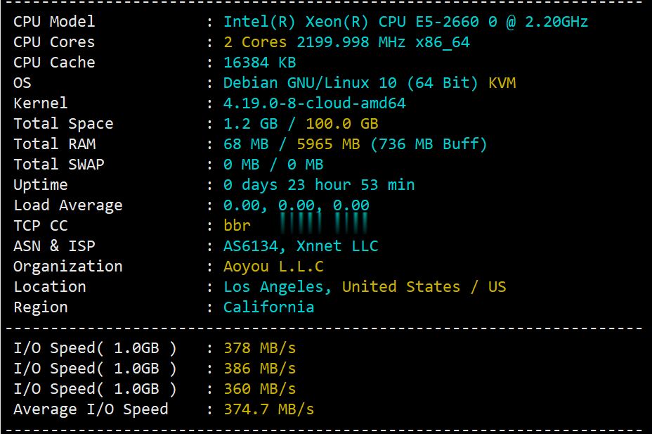
FBICDN,0.1元解决伪墙/假墙攻击,超500 Gbps DDos 防御,每天免费流量高达100G,免费高防网站加速服务
最近很多网站都遭受到了伪墙/假墙攻击,导致网站流量大跌,间歇性打不开网站。这是一种新型的攻击方式,攻击者利用GWF规则漏洞,使用国内服务器绑定host的方式来触发GWF的自动过滤机制,造成GWF暂时性屏蔽你的网站和服务器IP(大概15分钟左右),使你的网站在国内无法打开,如果攻击请求不断,那么你的网站就会是一个一直无法正常访问的状态。常规解决办法:1,快速备案后使用国内服务器,2,使用国内免备案服...
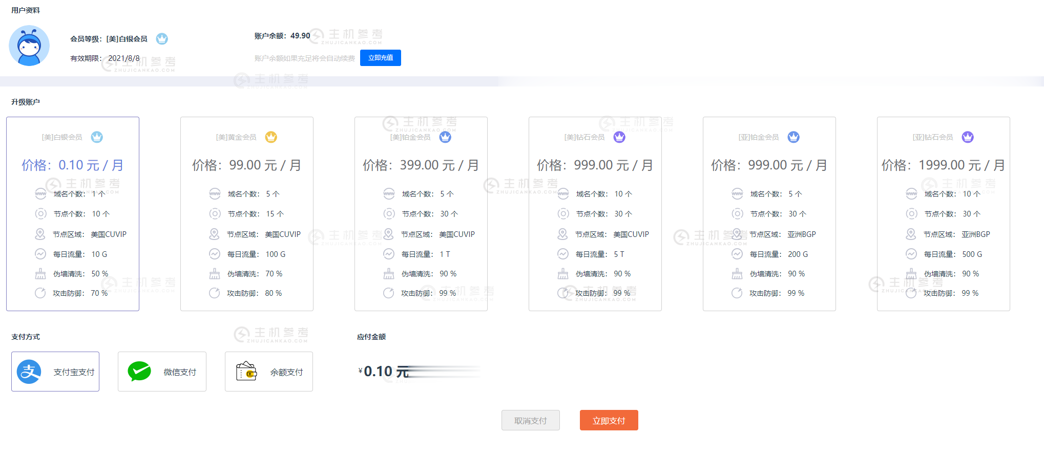
弘速云(28元/月)香港葵湾2核2G10M云服务器
弘速云怎么样?弘速云是创建于2021年的品牌,运营该品牌的公司HOSU LIMITED(中文名称弘速科技有限公司)公司成立于2021年国内公司注册于2019年。HOSU LIMITED主要从事出售香港vps、美国VPS、香港独立服务器、香港站群服务器等,目前在售VPS线路有CN2+BGP、CN2 GIA,该公司旗下产品均采用KVM虚拟化架构。可联系商家代安装iso系统,目前推出全场vps新开7折,...

7xxuu.com为你推荐
-
百度关键词工具常见百度关键词挖掘方法分别是什么请列举?百度指数词百度指数是指,词不管通过什么样的搜索引擎进行搜索,都会被算成百度指数吗?www.03ggg.comwww.tvb33.com这里好像有中国性戏观看吧??dadi.tvapple TV 功能介绍www.gogo.comNEO春之色直径?dpscycle魔兽世界国服,求几个暗影MS的输出宏网页源代码什么是网页源代码!打开网页后怎么找?4399宠物连连看2.54399游戏里的宠物连连看3.1版本,电脑网页有,为什么手机里没有呢?我想下这个版本在手机上,因为恶魔兜兜恶魔圈怎么选癫狂莱姿蔓圣诗蔓有祛痘功效吗