Conditionfastreport2.5
fastreport2.5 时间:2021-05-24 阅读:()
SemiconductorComponentsIndustries,LLC,2012November,2012Rev.
01PublicationOrderNumber:NB3L14S/DNB3L14S2.
5V1:4LVDSFanoutBufferTheNB3L14Sisadifferential1:4LVDSClockfanoutbuffer.
Thedifferentialinputsincorporateinternal50WterminationresistorsthatareaccessedthroughtheVTpin.
TheNB3L14SLVDSsignalswillbebufferedandreplicatedtoidenticalLVDScopiesoftheInputoperatingupto300MHz.
Assuch,theNB3L14SisidealforClockdistributionapplicationsthatrequirelowskew.
TheNB3L14Sisofferedinasmall3mmx3mm16QFNpackage.
Applicationnotes,models,andsupportdocumentationareavailableatwww.
onsemi.
com.
FeaturesMaximumInputClockFrequency;300MHzLowOutputtoOutputSkew;20ps450psTypicalPropagationDelay250psTypicalRiseandFallTimesSinglePowerSupply;VCC=2.
5$5%ThesearePbFreeDevicesA=AssemblyLocationL=WaferLotY=YearW=WorkWeekG=PbFreePackage*Foradditionalmarkinginformation,refertoApplicationNoteAND8002/D.
MARKINGDIAGRAM*QFN16MNSUFFIXCASE485Ghttp://onsemi.
comSeedetailedorderingandshippinginformationinthepackagedimensionssectiononpage7ofthisdatasheet.
ORDERINGINFORMATION16NB3L14SALYWGG1Figure1.
LogicDiagram(Note:Microdotmaybeineitherlocation)1Q3Q3Q2Q2Q1Q1Q0Q050W50WINVTINVCCVCCNB3L14Shttp://onsemi.
com2Figure2.
NB3L14SPinout,16pinQFN(TopView)Q3Q3VCCGNDINVTNCINQ1Q1Q2Q256781615141312111091234NB3L14SExposedPad(EP)Q0Q0VCCVCCIN*IN*Q010101xx0(Note1)1.
Outputswillbeattheknownstateinthistableatinitialpowerup.
Theoutputswillalsobeattheknownstateduringnormaloperationwheninputsareleftopen.
*DefaultshighwhenleftopenTable1.
TRUTHTABLEQ101(Note1)Table2.
PINDESCRIPTIONPinNameI/ODescription1Q1LVDSOutputNoninvertedINoutput.
Typicallyloadedwith100Wreceiverterminationresistoracrossdifferentialpair.
2Q1LVDSOutputInvertedINoutput.
Typicallyloadedwith100Wreceiverterminationresistoracrossdifferentialpair.
3Q2LVDSOutputNoninvertedINoutput.
Typicallyloadedwith100Wreceiverterminationresistoracrossdifferentialpair.
4Q2LVDSOutputInvertedINoutput.
Typicallyloadedwith100Wreceiverterminationresistoracrossdifferentialpair.
5Q3LVDSOutputNoninvertedINoutput.
Typicallyloadedwith100Wreceiverterminationresistoracrossdifferentialpair.
6Q3LVDSOutputInvertedINoutput.
Typicallyloadedwith100Wreceiverterminationresistoracrossdifferentialpair.
7VCCPositiveSupplyVoltage.
8VCCPositiveSupplyVoltage.
9INLVDSInvertedDifferentialInput;pinwilldefaultHIGHwhenleftopen10NCNoConnectThisisnotconnected.
11VTInputTerminationInternal100WCentertappedTerminationPinforINandIN,leaveopenforLVDS.
12INLVDSNoninvertedDifferentialInput;pinwilldefaultHIGHwhenleftopen.
13GNDNegativeSupplyVoltage.
14VCCPositiveSupplyVoltage.
15Q0LVDSOutputNoninvertedINoutput.
Typicallyloadedwith100Wreceiverterminationresistoracrossdifferentialpair.
16Q0LVDSOutputInvertedINoutput.
Typicallyloadedwith100Wreceiverterminationresistoracrossdifferentialpair.
EPTheExposedPad(EP)ontheQFN16packagebottomisthermallyconnectedtothedieforimprovedheattransferoutofpackage.
Theexposedpadmustbeattachedtoaheatsinkingconduit.
Thepadiselectricallyconnectedtothedie,andisrequiredtobeelectricallyandthermallyconnectedtoGNDonthePCboard.
NB3L14Shttp://onsemi.
com3Table3.
ATTRIBUTESCharacteristicsValueMoistureSensitivity(Note2)Level1FlammabilityRatingOxygenIndex:28to34UL94V0@0.
125inInputPullupResistorstoVCConInputs200kWESDProtectionHumanBodyModelMachineModel>4kV>200VTransistorCount440MeetsorexceedsJEDECSpecEIA/JESD78ICLatchupTest2.
Foradditionalinformation,seeApplicationNoteAND8003/D.
Table4.
MAXIMUMRATINGSSymbolParameterCondition1Condition2RatingUnitVCCPositivePowerSupplyGND=0V4.
6VVINPositiveInputGND=0VVIN≤VCC4.
6VIINInputCurrentThroughRT(50WResistor)StaticSurge3570mAmAIOSCOutputShortCircuitCurrentLinetoLine(QtoQ)LinetoGND(QorQtoGND)QorQQtoQtoGNDContinuousContinuous1224mATAOperatingTemperatureRangeQFN1640to+85°CTstgStorageTemperatureRange65to+150°CqJAThermalResistance(JunctiontoAmbient)(Note3)0lfpm500lfpmQFN16QFN1641.
635.
2°C/W°C/WqJCThermalResistance(JunctiontoCase)1S2P(Note3)QFN164.
0°C/WTsolWaveSolderPbFree265°CStressesexceedingMaximumRatingsmaydamagethedevice.
MaximumRatingsarestressratingsonly.
FunctionaloperationabovetheRecommendedOperatingConditionsisnotimplied.
ExtendedexposuretostressesabovetheRecommendedOperatingConditionsmayaffectdevicereliability.
3.
JEDECstandardmultilayerboard1S2P(1signal,2power)with8filledthermalviasunderexposedpad.
NB3L14Shttp://onsemi.
com4Table5.
DCCHARACTERISTICSVCC=2.
375Vto2.
625V,GND=0V,TA=40°Cto+85°CSymbolCharacteristicMinTypMaxUnitICCPowerSupplyCurrent(Note4)4565mADIFFERENTIALINPUTSDRIVENDIFFERENTIALLY(Figures4,8,and9)(Note5)VIHDDifferentialInputHIGHVoltage11501800mVVILDDifferentialInputLOWVoltageGNDVIHD150mVVCMRInputCommonModeRange(DifferentialConfiguration)(Note6)751725mVVIDDifferentialInputVoltage(VIHDVILD)1501800mVRTINInternalInputTerminationResistor405060WLVDSOUTPUTS(Note7)VODDifferentialOutputVoltage(SingleEndedMeasurement)250350450mVDVODChangeinMagnitudeofVODforComplementaryOutputStates(Note8)0125mVVOSOffsetVoltage(Figure7)112512501375mVDVOSChangeinMagnitudeofVOSforComplementaryOutputStates(Note8)0125mVVOHOutputHIGHVoltage(Note9)14251600mVVOLOutputLOWVoltage(Note10)9001075mVNOTE:Devicewillmeetthespecificationsafterthermalequilibriumhasbeenestablishedwhenmountedinatestsocketorprintedcircuitboardwithmaintainedtransverseairflowgreaterthan500lfpm.
Electricalparametersareguaranteedonlyoverthedeclaredoperatingtemperaturerange.
Functionaloperationofthedeviceexceedingtheseconditionsisnotimplied.
Devicespecificationlimitvaluesareappliedindividuallyundernormaloperatingconditionsandnotvalidsimultaneously.
4.
Inputpins,IN=300mV,IN=1V.
OutputpinsloadedwithRL=100Wacrosstheoutputs.
5.
VIHD,VILD,VIDandVCMRparametersmustbecompliedwithsimultaneously.
6.
VCMRminvaries1:1withGND,VCMRmaxvaries1:1withVCC.
TheVCMRrangeisreferencedtothemostpositivesideofthedifferentialinputsignal.
7.
LVDSoutputsrequire100Wreceiverterminationresistorbetweendifferentialpair.
SeeFigure6.
8.
Parameterguaranteedbydesignverificationnottestedinproduction.
9.
VOHmax=VOSmax+VODmax.
10.
VOLmax=VOSminVODmax.
NB3L14Shttp://onsemi.
com5Table6.
ACCHARACTERISTICS(VCC=2.
375Vto2.
625V,GND=0V)SymbolCharacteristic40°Cto+85°CUnitMinTypMaxfinMaxMaximumInputClockFrequency300MHzVOUTPPOutputVoltageAmplitude(@VINPPmin)fin≤300MHz250350450mVtPLH,tPHLDifferentialInputtoDifferentialOutput,INtoQPropagationDelay@50MHz300450600pstSKEWWithinDeviceOutputtoOutputSkew(Note12)DevicetoDeviceSkew(Note12)53020200psVINPPInputVoltageSwing/Sensitivity(DifferentialConfiguration)(Note11)1501800mVtrtfOutputRise/FallTimes@50MHzQ,Q(20%80%)250350psNOTE:Devicewillmeetthespecificationsafterthermalequilibriumhasbeenestablishedwhenmountedinatestsocketorprintedcircuitboardwithmaintainedtransverseairflowgreaterthan500lfpm.
Electricalparametersareguaranteedonlyoverthedeclaredoperatingtemperaturerange.
Functionaloperationofthedeviceexceedingtheseconditionsisnotimplied.
Devicespecificationlimitvaluesareappliedindividuallyundernormaloperatingconditionsandnotvalidsimultaneously.
11.
Inputvoltageswingisasingleendedmeasurementoperatingindifferentialmode.
12.
Skewismeasuredbetweenoutputsunderidenticaltransition@50MHz.
INPUTCLOCKFREQUENCY(MHz)Figure3.
OutputVoltageAmplitude(VOUTPP)versusInputClockFrequency(fin)andTemperature(@VCC=2.
5V)OUTPUTVOLTAGEAMPLITUDE(mV)0501001502002503003504001002003000400NB3L14Shttp://onsemi.
com6LVDSDriverIN50WZo=50WZo=50W50WINVT=OPENGNDGNDNB3L14SVCC=3.
3Vor2.
5VVCC=2.
5VFigure4.
LVDSInterfaceFigure5.
ACReferenceMeasurementININQQtPHLtPLHVINPP=VIH(IN)VIL(IN)VOUTPP=VOH(Q)VOL(Q)Figure6.
TypicalLVDSTerminationforOutputDriverandDeviceEvaluationDriverDeviceOscilloscopeQDQDLVDS100WZo=50WZo=50WHIZProbeHIZProbeVOLQNVOHQNVOSVODFigure7.
LVDSOutputFigure8.
DifferentialInputsDrivenDifferentiallyININNB3L14Shttp://onsemi.
com7VILD(MAX)VIHD(MAX)VIHDVILDVIHD(MIN)VILD(MIN)VCMRGNDFigure9.
VCMRDiagramVID=VIHDVILDVCCVCMRmaxVCMRminFigure10.
TapeandReelPin1QuadrantOrientationORDERINGINFORMATIONDevicePackageShippingNB3L14SMNGQFN16,3X3mm(PbFree)123Units/RailNB3L14SMNTXGQFN16,3X3mm(PbFree)3000/Tape&Reel(Pin1OrientationinQuadrantB,Figure10)Forinformationontapeandreelspecifications,includingpartorientationandtapesizes,pleaserefertoourTapeandReelPackagingSpecificationsBrochure,BRD8011/D.
NB3L14Shttp://onsemi.
com8PACKAGEDIMENSIONSQFN163x3,0.
5PCASE485GISSUEF16XSEATINGPLANELDE0.
10CAA1eD2E2b148916NOTES:1.
DIMENSIONINGANDTOLERANCINGPERASMEY14.
5M,1994.
2.
CONTROLLINGDIMENSION:MILLIMETERS.
3.
DIMENSIONbAPPLIESTOPLATEDTERMINALANDISMEASUREDBETWEEN0.
25AND0.
30MMFROMTERMINAL.
4.
COPLANARITYAPPLIESTOTHEEXPOSEDPADASWELLASTHETERMINALS.
BA0.
10CTOPVIEWSIDEVIEWBOTTOMVIEWPIN1LOCATION0.
05C0.
05C(A3)CNOTE416X0.
10C0.
05CABNOTE3K16XL1DETAILALALTERNATETERMINALCONSTRUCTIONSA1A3LDETAILBMOLDCMPDEXPOSEDCuALTERNATECONSTRUCTIONSDETAILADETAILB*ForadditionalinformationonourPbFreestrategyandsolderingdetails,pleasedownloadtheONSemiconductorSolderingandMountingTechniquesReferenceManual,SOLDERRM/D.
RECOMMENDED2X0.
50PITCH1.
843.
301DIMENSIONS:MILLIMETERS0.
5816X2X0.
3016XOUTLINEPACKAGE2X2X0.
10CABe/2SOLDERINGFOOTPRINT*DIMMINNOMMAXMILLIMETERSA0.
800.
901.
00A10.
000.
030.
05A30.
20REFb0.
180.
240.
30D3.
00BSCD21.
651.
751.
85E3.
00BSCE21.
651.
751.
85e0.
50BSCK0.
18TYPL0.
300.
400.
50L10.
000.
080.
15ONSemiconductorandareregisteredtrademarksofSemiconductorComponentsIndustries,LLC(SCILLC).
SCILLCownstherightstoanumberofpatents,trademarks,copyrights,tradesecrets,andotherintellectualproperty.
AlistingofSCILLC'sproduct/patentcoveragemaybeaccessedatwww.
onsemi.
com/site/pdf/PatentMarking.
pdf.
SCILLCreservestherighttomakechangeswithoutfurthernoticetoanyproductsherein.
SCILLCmakesnowarranty,representationorguaranteeregardingthesuitabilityofitsproductsforanyparticularpurpose,nordoesSCILLCassumeanyliabilityarisingoutoftheapplicationoruseofanyproductorcircuit,andspecificallydisclaimsanyandallliability,includingwithoutlimitationspecial,consequentialorincidentaldamages.
"Typical"parameterswhichmaybeprovidedinSCILLCdatasheetsand/orspecificationscananddovaryindifferentapplicationsandactualperformancemayvaryovertime.
Alloperatingparameters,including"Typicals"mustbevalidatedforeachcustomerapplicationbycustomer'stechnicalexperts.
SCILLCdoesnotconveyanylicenseunderitspatentrightsnortherightsofothers.
SCILLCproductsarenotdesigned,intended,orauthorizedforuseascomponentsinsystemsintendedforsurgicalimplantintothebody,orotherapplicationsintendedtosupportorsustainlife,orforanyotherapplicationinwhichthefailureoftheSCILLCproductcouldcreateasituationwherepersonalinjuryordeathmayoccur.
ShouldBuyerpurchaseoruseSCILLCproductsforanysuchunintendedorunauthorizedapplication,BuyershallindemnifyandholdSCILLCanditsofficers,employees,subsidiaries,affiliates,anddistributorsharmlessagainstallclaims,costs,damages,andexpenses,andreasonableattorneyfeesarisingoutof,directlyorindirectly,anyclaimofpersonalinjuryordeathassociatedwithsuchunintendedorunauthorizeduse,evenifsuchclaimallegesthatSCILLCwasnegligentregardingthedesignormanufactureofthepart.
SCILLCisanEqualOpportunity/AffirmativeActionEmployer.
Thisliteratureissubjecttoallapplicablecopyrightlawsandisnotforresaleinanymanner.
PUBLICATIONORDERINGINFORMATIONN.
AmericanTechnicalSupport:8002829855TollFreeUSA/CanadaEurope,MiddleEastandAfricaTechnicalSupport:Phone:421337902910JapanCustomerFocusCenterPhone:81358171050NB3L14S/DAnyLevelandECLinPSMAXaretrademarksofSemiconductorComponentsIndustries,LLC(SCILLC).
LITERATUREFULFILLMENT:LiteratureDistributionCenterforONSemiconductorP.
O.
Box5163,Denver,Colorado80217USAPhone:3036752175or8003443860TollFreeUSA/CanadaFax:3036752176or8003443867TollFreeUSA/CanadaEmail:orderlit@onsemi.
comONSemiconductorWebsite:www.
onsemi.
comOrderLiterature:http://www.
onsemi.
com/orderlitForadditionalinformation,pleasecontactyourlocalSalesRepresentative
- Conditionfastreport2.5相关文档
- khrfastreport2.5
- ROUTfastreport2.5
- RATINGSfastreport2.5
- DOCUMENTATIONfastreport2.5
- TMAXfastreport2.5
- 组件fastreport2.5
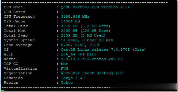
ShockHosting日本机房VPS测试点评
这个月11号ShockHosting发了个新上日本东京机房的邮件,并且表示其他机房可以申请转移到日本,刚好赵容手里有个美国的也没数据就发工单申请新开了一个,这里做个简单的测试,方便大家参考。ShockHosting成立于2013年,目前提供的VPS主机可以选择11个数据中心,包括美国洛杉矶、芝加哥、达拉斯、杰克逊维尔、新泽西、澳大利亚、新加坡、日本、荷兰和英国等。官方网站:https://shoc...
Sparkedhost($8/月)美国迈阿密AMD Ryzen高性能VPS;免费100G高防
sparkedhost怎么样?sparkedhost主机。Sparkedhost于2017年7月注册在美国康涅狄格州,2018年收购了ClynexHost,2019年8月从Taltum Solutions SL收购了The Beast Hosting,同年10月从Reilly Bauer收购了OptNode Hosting。sparkedhost当前的业务主要为:为游戏“我的世界”提供服务器、虚拟...

80VPS:香港服务器月付420元;美国CN2 GIA独服月付650元;香港/日本/韩国/美国多IP站群服务器750元/月
80vps怎么样?80vps最近新上了香港服务器、美国cn2服务器,以及香港/日本/韩国/美国多ip站群服务器。80vps之前推荐的都是VPS主机内容,其实80VPS也有独立服务器业务,分布在中国香港、欧美、韩国、日本、美国等地区,可选CN2或直连优化线路。如80VPS香港独立服务器最低月付420元,美国CN2 GIA独服月付650元起,中国香港、日本、韩国、美国洛杉矶多IP站群服务器750元/月...

fastreport2.5为你推荐
-
第一届全国技能大赛山东省选拔赛交换机route支持ipad支持ipadDescriptionios5iexplore.exe应用程序错误iexplore.exe应用程序错误canvas2动漫cv井口裕香,都有哪些作品?iphonewifi为什么我的苹果手机连不上wifi联通iphone4联通iphone4合约联通合约机iphone5联通合约机iphone5和电信合约机Iphone5哪个好