layerslick
lick 时间:2021-01-09 阅读:()
1HighMobilityStrainedGermaniumQuantumWellFieldEffectTransistorastheP-ChannelDeviceOptionforLowPower(Vcc=0.
5V)III-VCMOSArchitectureR.
Pillarisetty,B.
Chu-Kung,S.
Corcoran,G.
Dewey,J.
Kavalieros,H.
Kennel,R.
Kotlyar,V.
Le,D.
Lionberger,M.
Metz,N.
Mukherjee,J.
Nah,W.
Rachmady,M.
Radosavljevic,U.
Shah,S.
Taft,H.
Then,N.
Zelick,andRChauIntelCorporation,TechnologyandManufacturingGroup,Hillsboro,OR97124,USAAbstractInthisarticlewedemonstrateaGep-channelQWFETwithscaledTOXE=14.
5andmobilityof770cm2/V*satns=5x1012cm-2(chargedensityinthestate-of-the-artSitransistorchannelatVcc=0.
5V).
ForthinTOXE<40,thisrepresentsthehighestholemobilityreportedforanyGedeviceandis4xhigherthanstate-of-the-artstrainedsilicon.
TheQWFETarchitectureachieveshighmobilitybyincorporatingbiaxialstrainandeliminatingdopantimpurityscattering.
ThethinTOXEwasachievedusingaSicapandalowDttransistorprocess,whichhasalowoxideinterfaceDit.
ParallelconductionintheSiGebufferwassuppressedusingaphosphorusjunctionlayer,allowinghealthysubthresholdslopeinGeQWFETforthefirsttime.
TheGeQWFETachievesanintrinsicGmsatwhichis2xhigherthantheInSbp-channelQWFET.
TheseresultssuggesttheGeQWFETisaviablep-channeloptionfornon-siliconCMOS.
IntroductionRecently,III-Vquantumwellfieldeffecttransistor(QWFET)researchforfuturelowpowerCMOSlogicapplicationshasmadesignificantprogress[1,3].
Whilen-channelIII-VstudieshaveshownsignificantdrivecurrentgainsoverstateoftheartsiliconatlowVcc[1],thecorrespondingp-channeltransistorwiththinTOXEandhighmobility()hasnotyetbeendemonstrated.
Inthisstudy,wedemonstrateahighmobilitystrainedgermanium(Ge)p-channelQWFETsuitableforlowpowerCMOSarchitecturewithscaledTOXE=14.
5andholemobility=770cm2/V*satns=5x1012cm-2.
ForTOXE<40,thisrepresentsthehighestholemobilityreportedforanyGedeviceandis4xhigherthanstate-of-the-artstrainedsilicon.
TheseresultssuggestthattheGeQWFETisaviablep-channeloptionforIII-VCMOSrealization.
MaterialsGrowthandDeviceFabricationFigure1showsaschematicofabiaxiallystrainedundopedGeQWstructure.
TheboronmodulationdopinglayerallowsforHallmeasurement,butisoptionalforimplantedS/Dtransistors.
ThephosphorusdopedlayerisgrowntosuppressparallelconductionintheSiGebuffers.
AcrosssectionalTEMimageofaGeQWgrownbyRTCVDon300mmsiliconisshowninFig2,highlightingboththe2-stepSiGebufferlayersandbiaxiallystrainedGeQWlayerboundedbySi.
3Ge.
7barriers.
Althoughnotshown,wealsogrewrelaxedGelayersonthistwolayerbuffertoprovideuswithaGeMOSFETreferencestructure.
Figure3showsX-raydiffractionspectraofthesymmetric(004)reflectionforboththeGeQWandrelaxedGestructuresindicating1.
3%biaxialstrainintheGeQW.
TheHallmobilityforRTCVDgrownGeQWstructures,plottedinFig4,matchesMBEgrownGeQWliteraturedata[5-7]andshowsgainovertheInSbQW[3]andstrainedSi[2].
Figure5showsaTEMofafullyprocessedGeQWFETutilizingshallowtrenchisolation(notshown),HfO2/TiNhigh-kmetalgate,self-alignedB-implantedS/D,W/Ticontacts,astrainedGeQWchannel,andaphosphorusisolationlayer.
ATEMimageofaGeQWFETwithanin-situdopedSixGe1-xraisedsource/drain(RSD)isshowninFig6.
SiliconCapandGateDielectricInterfaceAthinSicaplayerisrequiredtopreventcarrierspill-outfromtheGeQW.
ThisisdemonstratedinFig7wherek*p-Poissonsimulationsshowthatforaholedensity(ns)=5x1012cm-2,a10SicaplayerconfinescarriersintheGeQW,whereassignificantcarrierspill-outoccurswitha100Si.
3Ge.
7barrier.
Figure8showsaTEMimageofahigh-kmetalgatestackwithathinsiliconcaponaGeQW.
Partofthesiliconcapisoxidizedduetothermalcycle(Dt)duringthetransistorfabricationprocess.
ThisissuggestedbytheEDSdepthprofileofthegatestack,showninFig9,indicatingthepresenceofbothSiandSiO2betweentheGeandHfO2.
CVdatainFig10indicatesinversionTOXEreductionwithSicapthicknessscaling.
DuetoasymmetryofthevalenceandconductionbandoffsetsbetweenSiandGe,theSicaponlycontributestoCinv.
Hence,theSiO2thickness(TSiO2)ontheSicapcanbeextractedfromtheaccumulationTOXE,andinthisexampleis6forallcasesduetoconstantthermalDt.
SinceabodycontactisneededtomeasuretheaccumulationCV,thisdatawascollectedfromtheGeMOSFETreferencedevice.
ThecorrespondingvsnsplottedinFig11showsthatimprovesasSicapthicknessisreducedduetoreductionincarrierspill-out.
However,isdegradedsignificantlywithoutSicapduetoanincreaseininterfacetrapdensity(Dit).
Figure12showsthatbyloweringprocessDtfrom700°Cto635°CTOXEcanscaleto14.
5withoutlossofmobilityviaTSiO2reductionontheSicap.
GeQWFETDeviceAnalysisTheminimalCVfrequencydispersioninFig13indicatesagoodqualityinterfaceforboththerelaxedGeMOSFETreferenceandstrainedGeQWFETwiththesame14.
5TOXEprocess.
Figure14showsmobilityvsnsforbothdevices.
Theexperimentsagreewithk*psimulations,whichassumeDitandsurfaceroughnessmatchedtostate-of-the-artSi.
ThisindicatesahighqualityoxideinterfaceonGe.
Atns=5x1012cm-2,theQWFETexhibits4xmobilitygainoverstate-of-the-artstrainedSi[2].
Furthermore,inFig15theGeQWFETachievesthehighestmobility(770cm2/V*s)atthethinnestTOXE(14.
5)comparedtothebestGedevicesinliterature[8-9].
Figs16and17plotthetemperature(T)dependenceoftheGeQWFETmobility,whichshowsnosaturationofdowntoT=20K.
ThisindicatesminimalimpactfromCoulombscatteringduetoabsenceofdopingintheQWandlowDit.
2Figure18showsdraincurrentvsgatebias(Vg)atVds=-0.
5VforaGeQWFET,withLgate=100nm.
Thedeviceachieveshealthysubthresholdslope(SS)of97mV/DECforthefirsttimeinaGeQWstructure,duetothesuppressionofparallelconductionthroughtheSiGebufferusingthephosphorusisolationlayer.
Figure19plotstheSSvsgatelengthdependencefortheGeQWFETandshowsremovalofmodulationdoping(MD)improvesSCE.
Theraisedsource/drainprocessfurtherimprovesSCEbyallowingforreductionoreliminationofimplantation.
Figure20plotspeakintrinsicGmsatvsSS,showingtheintrinsicGmsatoftheGeQWFETwithRSDprocessis2xhigherthanthatoftheInSbp-channelQWFET[3].
TheRSDprocessexhibitsa35%improvementinintrinsicGmduetohighershortchannelstraincomparedtotheimplantonlyflow.
Figure21comparesIonvsIoffcharacteristicsoftheGeQWFETwithRSD(thiswork)tothebestreportedIII-V[3]andgermaniumdevices[10]atVcc=0.
5V.
TheseGeQWFETsexhibit2xhigherdrivecurrentforthesameIoff.
ConclusionAGep-channelQWFETwithscaledTOXE=14.
5andmobilityof770cm2/V*satns=5x1012cm-2(Vcc=0.
5V)hasbeenachieved.
ForTOXE<40,thisrepresentsthehighestholemobilityreportedforanyGedeviceandis4xhigherthanstate-of-the-artstrainedsilicon.
TheQWFETarchitectureachieveshighmobilitybyincorporatingbiaxialstrainandeliminatingdopantimpurityscattering.
ThethinTOXEwasachievedusingaSicapandalowDttransistorprocess,whichhasalowoxideinterfaceDit.
ParallelconductionintheSiGebufferwassuppressedusingaphosphorusjunctionlayer,allowinghealthysubthresholdslopeinGeQWFETforthefirsttime.
TheGeQWFETachievesanintrinsicGmsatwhichis2xhigherthantheInSbp-channelQWFET.
Furthermore,atVcc=0.
5V,theGeQWFETexhibits2xhigherdrivecurrentatfixedIoffthanthebestIII-V[3]andgermaniumdevices[10]reportedtodate.
References[1]G.
Deweyetal.
,IEDMTech.
Dig.
,pp.
487-490(2009).
[2]P.
Packanetal.
,IEDMTech.
Dig.
,pp.
3.
4.
1(2008).
[3]M.
Radosavljevicetal.
,IEDMTech.
Dig.
,pp.
30.
3.
1(2008).
[4]S.
Koesteretal.
,IEEEElecDevLett.
,vol.
21,pp110(2000).
[5]S.
Madhavietal.
,J.
Appl.
Phys.
,89,2497(2001).
[6]C.
M.
Engelhardtetal.
,Sol.
Stat.
Elec.
37,949(1994).
[7]T.
Irisawaetal.
,Jpn.
J.
Appl.
Phys.
,Part140,2694(2001).
[8]J.
Mitardetal.
,VLSITech.
Dig.
,pp.
82-83(2009).
[9]O.
Weberetal.
,IEDMTech.
Dig.
,pp.
137-140(2005).
[10]J.
Mitardetal.
,IEDMTech.
Dig.
,pp.
873-876(2008).
Fig1:SchematicofbiaxiallystrainedundopedGeQWstructureonasiliconsubstrate.
Front-sideorbacksideB-modulationdopingallowsforHallmeasurement,butisoptionalforimplantedS/Dtransistors.
PhosphoruslayerisusedtosuppressparallelconductionintheSiGebuffers.
Fig2:CrosssectionalTEMimageofaGeQWstructure,whichwasgrownbyRTCVDon300mmsilicon,showing(a)2-stepSiGebufferlayersand(b)BiaxiallystrainedGeQWlayerboundedbySi.
3Ge.
7barriers.
Fig3:HighresolutionX-raydiffractionspectraofthesymmetric(004)reflectionforbothstrainedGeQW(solid)andrelaxedGe(dash)structuresonsiliconsubstrate,indicating1.
3%biaxialstrainintheGeQW.
110100100010000-12000-9000-6000-30000Angle(arcsec)Intensity(cps)SiliconSi.
7Ge.
3Si.
3Ge.
7RelaxedGe1.
3%StrainedGeQW3Fig7:Valencebanddiagramandholewavefunctiondeterminedusingk*pPoissontechniqueforGeQWFETfor(a)100ASi.
3Ge.
7topbarrierand(b)10ASiCap.
Inbothcases,ns=5x1012cm-2(Vcc=0.
5V).
ThethinSicapconfinescarriersintheQWlayer.
Fig8:HighresolutioncrosssectionalTEMimageofahigh-kmetalgatestackwithathinSicaponaGeQWFET.
PartoftheSicapisoxidizedduetothermalDtduringthetransistorfabricationprocess.
Fig10:FullCVcharacteristicsofGeMOSFETreferenceshowinginversionTOXEreductionwithSicapthicknessscaling.
SincetheSicaponlycontributestoinversioncapacitance,theSiO2thickness(TSiO2)onthesiliconcapcanbeextractedfromtheaccumulationcapacitance.
Inthisexample,TSiO2=6AforallcasesduetoconstantthermalprocessDt.
Fig12:GeMOSFETcarriermobilityatns=5x1012cm-2vsTOXEfor635°C(circle)and700°C(triangle)processDt.
InbothcasesTOXEisscaledviaSicapthicknessreduction.
LowerDtenablesTOXEscalingdownto14.
5withoutmobilityloss,viareductioninTSiO2.
Fig5:CrosssectionalTEMimageofafullyprocessedGeQWFETdevicehighlightingthestrainedGeQWchannel,TiNgateelectrode,selfalignedimplantedS/D,W/TiS/Dcontacts,andthephosphorusisolationlayerthatsuppressesparallelconductionintheSiGebuffer.
Fig4:Hallmobilityvsdensityfor300mmRTCVDgrown1.
3%strainedGeQWstructures,whichexhibitmobilitymatchedtoMBEgrownGeQWliteraturedata[5-7],andmobilitygainsovertheInSbQW[3]andstrainedsilicon[2].
Fig11:MobilityvscarrierdensityforGeMOSFETreferencewithdifferentSicapthickness.
MobilityimproveswithreducingSicapthicknessduetoreductionincarrierspill-out.
MobilitydegradesseverelywithoutSicapduetohighDit.
Fig9:EnergydispersiveX-rayspectroscopydepthprofileofthehigh-kmetalgatestackonGeshowninFig7,indicatingthepresenceofbothSiandSiO2betweentheGeandHfO2.
ThisconfirmsthatpartoftheSicapisoxidizedduetothermalDtduringthetransistorprocess.
FurtherquantificationwasperformedusingelectricalmeasurementsasshowninFigs.
9-11.
SiO2+SiliconCapGermaniumHfO2TiN2nm0.
0E+005.
0E-071.
0E-061.
5E-062.
0E-062.
5E-063.
0E-06-1.
5-1.
0-0.
50.
00.
51.
01.
5Vg[V]C[F/cm2]SiliconCapThickness:f=1MHz691114146THFO2=20W/TiS/DContactW/TiS/DContactTiNGateILDPhosJunctionIsolationSi.
3Ge.
7Buffer100nmStrainedUndopedGeQWChannelImplantedS/DImplantedS/D010020030040050060070080002468101214RelativeDistance[nm]Intensity[a.
u.
]OEDSTiEDS/2GeEDS/2HfEDSSiEDSGermaniumTiNGateHfO2SiO2+SiCap050010001500200025000.
E+002.
E+124.
E+126.
E+128.
E+12HoleDensity(cm-2)Mobility(cm2/V*s)RTCVD1.
3%StrainedGeQW[ThisWork]StrainedSi[2]2%StrainedInSbQW[3][5][6][7]MBE1.
3%StrainedGeQW02550751001251501752002252500.
0E+005.
0E+121.
0E+131.
5E+132.
0E+13HoleDensity[cm-2]Mobility[cm2/V*s]NoSiliconCap141196Dit=1.
8x1011cm-2/eVDit=9.
0x1011cm-2/eV05010015020025030081012141618202224TOXE[]Mobility@ns=5x1012[cm2/V*s]700°CDtTSiO2=10635°CDtTSiO2=605101520-1-0.
8-0.
6-0.
4-0.
200.
2ValenceBandEnergy(eV)05E+181E+192E+190510152025HoleDensity(cm^-3)GeQWSi.
3Ge.
7SliliconSi.
3Ge.
7GeQWSi.
3Ge.
7(a)(b)DepthAlongStack[nm]Fig6:CrosssectionalTEMimagehighlightingthegatestackandsource/drainofaGeQWFETincorporatingain-situBdopedSi-xGe1-xraisedsource/drain(RSD)whichallowsforreduction/removaloftheS/Dimplantation.
40200400600800100012001400160018000100200300400500600700SS[mV/DEC]PeakIntrinsicGmsat[uS/um]2%StrainedInSbQWFET[3]1.
3%StrainedGeQWFETNORSD(THISWORK)1.
7%StrainedGeQWFET[4]Vds=-0.
5V1.
3%StrainedGeQWFETWITHRSD(THISWORK)Fig13:Capacitancevsgatevoltageatf=1,0.
3,0.
1,0.
03,and0.
01MHzforboththeGeMOSFETreferencedeviceandstrainedGeQWFETusingthesameSicap+high-kprocess.
BothdevicesexhibitminimalCVdispersionatTOXE=14.
5.
Fig15:MobilityvsTOXEatns=5x1012cm-2fortheGeMOSFETreferenceandtheGeQWFET.
TheGeQWFETachievesthehighestmobility(770cm2/V*s)atthethinnestTOXE(14.
5)comparedtothebestrelaxed[8]andstrained[9]Geliteraturedatatodate.
Fig16:MobilityvsholecarrierdensityinastrainedGeQWFETfortemperaturesranging(frombottom)295K,250K,200K,150K,100K,50K,and20K.
Themobilityimproves~3xwhencooledtoT=20K.
Fig17:MobilityvsTfortheundopedGeQWFETandfortherelaxeddopedGeMOSFET.
ThedatafromtheQWFETsystemindicatesnosaturationofmobilitydowntoT=20K,indicatingminimalimpactfromCoulombscatteringduetoabsenceofdopingintheQWandlowDit.
Fig18:DraincurrentvsVgforaGeQWFETwithLgate=100nm,atVds=-0.
05V(opencircle)and-0.
5V(solidcircle).
Thedeviceexhibitsahealthysubthresholdslope(SS)=97mV/DECenabledbythephosphorusjunctionlayer,whichsuppressesparallelconductionthroughtheSiGebuffer.
Fig20:PeakintrinsicGmsatvssubthresholdslopeatVds=-0.
5VforthestrainedGeQWFETwithandwithoutRSD.
Includedintheplotarethestate-of-the-artInSbp-QWFET[3]andGeQWFET[4]intheliterature.
Fig14:MobilityvsnsforthestrainedGeQWFETandrelaxedGeMOSFETreference,withTOXE=14.
5.
Theexperimentaldatamatch6-bandk*psimulationsassumingDitandsurfaceroughnessmatchedtostate-of-the-artSi.
Atns=5x1012cm-2,theQWFETexhibits4xgainoverstate-of-the-artstrainedSi[2]0.
0E+005.
0E-071.
0E-061.
5E-062.
0E-062.
5E-063.
0E-06-2-1012Vg(V)C/A(F/cm)GeMOSFETTOXE=14.
5StrainedGeQWTOXE=14.
510kHZto1MHZ05001000150020002500300035000.
0E+005.
0E+121.
0E+131.
5E+13HoleDensity(cm-2)Mobility(cm2/Vs)T=295Kto20K1.
3%StrainedUndopedGeQW(TOXE=14.
5)RelaxedGeMOSFET(1e18)1.
3%StrainedUndopedGeQW3000600ns=5x1012cm-21x1013cm-21x1013cm-25x1012cm-21.
E-091.
E-081.
E-071.
E-061.
E-051.
E-041.
E-03-0.
5-0.
2500.
250.
5Vg[V]DrainCurrent[A/um]Vds=-0.
05VWithPhosJunctionNoPhosJunctionVds=-0.
5V0200400600800100012000.
0E+005.
0E+121.
0E+131.
5E+13HoleDensity(cm-2)Mobility(cm2/V*s)1.
3%StrainedGeQW(Undoped)RelaxedGeMOSFET(1e18)4xSolid=ExperimentOpen=SimulationStrainedSilicon[2]01002003004005006007008008101214161820222426TOXE[A]Mobility@ns=5x10¹²[cm2/V*s]1.
3%StrainedUndopedGeQW(THISWORK)RelaxedGeMOSFET(1e18)LiteratureDatatoDate[8][9]Fig19:SSvsgatelengthdependencefortheGeQWFETshowsremovalofmodulationdoping(MD)improvesSCE(diamond).
Theraisedsource/drainprocessfurtherimprovesSCEbyallowingforreduction(triangle)orelimination(circle)ofimplantation.
1.
E-081.
E-071.
E-061.
E-051.
E-0400.
10.
20.
30.
4Idsat[mA/um]Ioff[A/um]2%StrainedInSbQWFET[3]Vcc=0.
5V1.
3%StrainedGeQWFETWITHRSD(THISWORK)RelaxedGeMOSFET[10]Fig21:IonvsIoffforthestrainedGeQWFETwithRSDforVcc=0.
5V.
IncludedintheplotarethebestInSbp-QWFET[3]andshortchannelGeMOSFETdataintheliterature[10].
VGOFF=Vt+.
125VVGON=Vt-.
375V5010015020025030035040045050000.
050.
10.
150.
20.
250.
3GateLength[um]SS[mV/DEC]
- layerslick相关文档
- shortlick
- weighedlick
- Ealinglick
- ticipantslick
- informationinoneormoreareaslick
- subjectinglick
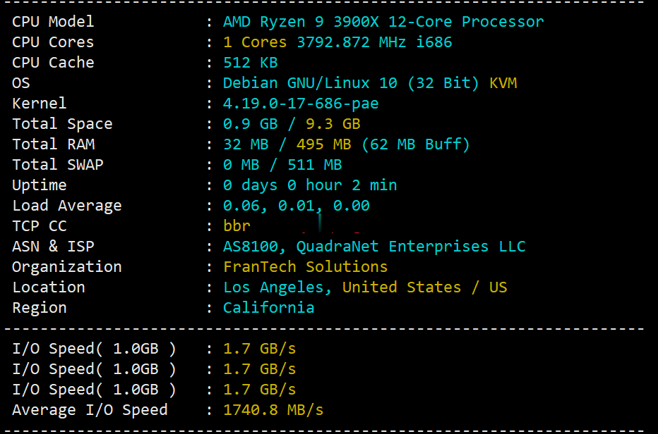
buyvm迈阿密机房VPS国内首发测评,高性能平台:AMD Ryzen 9 3900x+DDR4+NVMe+1Gbps带宽不限流量
buyvm的第四个数据中心上线了,位于美国东南沿海的迈阿密市。迈阿密的VPS依旧和buyvm其他机房的一样,KVM虚拟,Ryzen 9 3900x、DDR4、NVMe、1Gbps带宽、不限流量。目前还没有看见buyvm上架迈阿密的block storage,估计不久也会有的。 官方网站:https://my.frantech.ca/cart.php?gid=48 加密货币、信用卡、PayPal、...
天上云月付572元,起香港三网CN2直连,独立服务器88折优惠,香港沙田机房
天上云怎么样?天上云隶属于成都天上云网络科技有限公司,是一家提供云服务器及物理服务器的国人商家,目前商家针对香港物理机在做优惠促销,香港沙田机房采用三网直连,其中电信走CN2,带宽为50Mbps,不限制流量,商家提供IPMI,可以自行管理,随意安装系统,目前E3-1225/16G的套餐低至572元每月,有做大规模业务的朋友可以看看。点击进入:天上云官方网站天上云香港物理机服务器套餐:香港沙田数据中...

LOCVPS新上韩国KVM,全场8折,2G内存套餐月付44元起_网络传真服务器
LOCVPS(全球云)发布了新上韩国机房KVM架构主机信息,提供流量和带宽方式,适用全场8折优惠码,优惠码最低2G内存套餐月付仅44元起。这是一家成立较早的国人VPS服务商,目前提供洛杉矶MC、洛杉矶C3、和香港邦联、香港沙田电信、香港大埔、日本东京、日本大阪、新加坡、德国和荷兰等机房VPS主机,基于KVM或者XEN架构。下面分别列出几款韩国机房KVM主机配置信息。韩国KVM流量型套餐:KR-Pl...

lick为你推荐
-
海外主机租用怎么选择优质的国外服务器租用商!美国虚拟空间美国虚拟主机无限空间是什么意思?cm域名注册什么是CM域名?.cm .cm域名域名主机域名,主机空间和网站文件三者之间的区别是什么免费域名空间哪个免费空间的域名最好虚拟主机评测网求推荐一些适合个人博客网站的虚拟主机的服务商虚拟主机控制面板虚拟主机控制面板是什么?虚拟主机软件虚拟主机管理软件那个最好用?华众虚拟主机管理系统华众虚拟主机管理系统怎么样?域名网怎么样申请网站域名?