Minimum网站加v
网站加v 时间:2021-05-05 阅读:()
TPSM416254-Vto16-VInput,25-ADC/DCPowerModulewithCurrentSharing1FeaturesIntegratedinductorpowersolution11-mm*16-mm*4.
2-mmQFNpackage–AllpinsaccessiblefrompackageperimeterInputvoltagerange:4Vto16VWide-outputvoltagerange:0.
6Vto7.
1VSelectableinternalreference(±0.
5%accuracy)Stackableuptotwodevices–Paralleloutputsforhighercurrent–Phase-interleavingforreducedrippleEfficienciesupto97%Adjustablefixedswitchingfrequency(300kHzto1MHz)AllowssynchronizationtoanexternalclockAdvancedcurrentmodeprovidesultra-fastloadstepresponsePower-goodoutputMeetsEN55011radiatedEMIlimitsOperatingambientrange:–40°Cto+105°COperatingICjunctionrange:–40°Cto+125°CPincompatiblewith:15-ATPSM41615CreateacustomdesignusingtheTPSM41625WiththeWEBENCHPowerDesigner2ApplicationsTelecomandwirelessinfrastructureIndustrialautomatedtestequipmentEnterpriseswitchingandstorageapplicationsHigh-densitydistributedpowersystems3DescriptionTheTPSM41625powermoduleisaneasy-to-useintegratedpowersupplythatcombinesaDC/DCconverterwithpowerMOSFETs,ashieldedinductor,andpassivesintoacompactQFNpackage.
Thispowersolutionrequiresfewexternalcomponentswhilemaintainingtheabilitytoadjustkeyparameterstomeetspecificdesignrequirements.
ApplicationsrequiringincreasedcurrentcanbenefitfromtheabilitytoparalleltwoTPSM41625devices.
The11-mm*16-mm*4.
2-mm,69-pinQFNpackagewithoptimalpackagelayouthasexcellentpowerdissipationcapabilitywhichenhancesthermalperformance.
Thepackagefootprinthasallsignalpinsaccessiblefromtheperimeterandlargethermalpadsbeneaththedevice.
TheTPSM41625offersflexibiltywithmanyfeaturesincludingpowergoodsignal,clocksynchronization,programmableUVLO,soft-starttimingselection,prebiasstart-up,aswellasovercurrentandovertemperatureprotectionmakingitagreatproductforpoweringawiderangeofdevicesandsystems.
DeviceInformationDEVICENUMBERPACKAGE(1)BODYSIZE(NOM)TPSM41625QFN(69)11mm*16mm(1)Forallavailablepackages,seetheorderableaddendumattheendofthedatasheet.
spacespacespaceSimplifiedSchematicTypicalEfficiencywww.
ti.
comTPSM41625SLVSEW0A–SEPTEMBER2020–REVISEDDECEMBER2020Copyright2020TexasInstrumentsIncorporatedSubmitDocumentFeedback1ProductFolderLinks:TPSM41625TPSM41625SLVSEW0A–SEPTEMBER2020–REVISEDDECEMBER2020AnIMPORTANTNOTICEattheendofthisdatasheetaddressesavailability,warranty,changes,useinsafety-criticalapplications,intellectualpropertymattersandotherimportantdisclaimers.
PRODUCTIONDATA.
TableofContents1Features.
12Applications.
13Description.
14RevisionHistory.
25PinConfigurationandFunctions.
36Specifications.
56.
1AbsoluteMaximumRatings56.
2ESDRatings56.
3RecommendedOperatingConditions66.
4ThermalInformation66.
5ElectricalCharacteristics76.
6TypicalCharacteristics(PVIN=12V)96.
7TypicalCharacteristics(PVIN=5V)117DetailedDescription.
127.
1Overview.
127.
2FunctionalBlockDiagram.
127.
3FeatureDescription.
137.
4DeviceFunctionalModes.
218ApplicationandImplementation.
228.
1ApplicationInformation.
228.
2TypicalApplication.
229PowerSupplyRecommendations.
2410Layout.
2510.
1LayoutGuidelines.
2510.
2LayoutExamples.
2511DeviceandDocumentationSupport.
2811.
1DeviceSupport.
2811.
2ReceivingNotificationofDocumentationUpdates.
.
2811.
3SupportResources.
2811.
4Trademarks.
2811.
5ElectrostaticDischargeCaution.
2811.
6Glossary.
2812Mechanical,Packaging,andOrderableInformation.
294RevisionHistoryNOTE:Pagenumbersforpreviousrevisionsmaydifferfrompagenumbersinthecurrentversion.
ChangesfromRevision*(September2020)toRevisionA(December2020)PageChangeddevicestatusfromAdvanceInformationtoProductionData.
1TPSM41625SLVSEW0A–SEPTEMBER2020–REVISEDDECEMBER2020www.
ti.
com2SubmitDocumentFeedbackCopyright2020TexasInstrumentsIncorporatedProductFolderLinks:TPSM416255PinConfigurationandFunctionsFigure5-1.
69-PinQFNMOVPackage(TopView)Table5-1.
PinFunctionsPINTYPE(1)DESCRIPTIONNAMENO.
AGND19GAnalogground.
Zerovoltagereferenceforinternalreferencesandlogic.
DonotconnectthispintoPGND;theconnectionismadeinternaltothedevice.
BP521,22OOutputofaninternal5-Vregulatorusedforthecontrollerdriverstagewithinthemodule.
ThisoutputcanbeusedtoconnectapullupresistortothePGOODpin.
LeavethesepinsopenifnotusedasapullupforPGOOD.
DNC38,40–DoNotConnect.
DonotconnectthesepinstoAGND,PGND,anotherDNCpin,oranyothervoltage.
Thesepinsareconnectedtointernalcircuitry.
Eachpinmustbesolderedtoanisolatedpad.
EN25IEnablepin.
Thispinturnstheconverteronwhenfloatedoropened.
ThispinisinternallypulleduptotheBP5voltagewhenleftopen.
Theconvertercanbeturnedoffbyeitherdrivingitdirectlywithalogicinputoranopendrain/collectordevicetoconnectthispintoAGND.
Anexternalvoltagedividercanbeplacedbetweenthispin,AGND,andPVIN/VINtocreateanexternalUVLO.
ILIM20ICurrentlimitsettingpin.
Thispinsetsthecurrentlimitthresholdoftheconverter.
Leavethispinopenforthefullcurrentlimitthreshold.
ThecurrentlimitthresholdcanbeloweredbyconnectinganappropriateresistorfromthispintoAGND.
ISHARE23OCurrentsharingpin.
Thispinisinterconnectedbetweenmodulesformulti-phaseconfigurations.
Leavethispinopenforsingle-phaseconfigurations.
www.
ti.
comTPSM41625SLVSEW0A–SEPTEMBER2020–REVISEDDECEMBER2020Copyright2020TexasInstrumentsIncorporatedSubmitDocumentFeedback3ProductFolderLinks:TPSM41625Table5-1.
PinFunctions(continued)PINTYPE(1)DESCRIPTIONNAMENO.
MODE31IModeselectpin.
Thispinisusedtoconfigurethemoduleforsingle-phaseormulti-phaseoperation.
Forsingle-phaseoperation,thispinisusedtoselecttheAPIandBodyBrakefunctions.
Formulti-phaseoperation,thispinselectstheprimary/secondaryandSYNCconfigurations.
NC39,41,45-52–Notconnected.
Thesepinsarenotconnectedtoanycircuitrywithinthemodule.
ItisrecommendedthatthesepinsbeconnectedtothePGNDplaneontheapplicationboardtoenhanceshieldingandthermalperformance.
PGND8-11,17,18,34,37,53-58,68GThisisthereturnpathforthepowerstageofthedevice.
Connectthesepinstotheinputsupplyreturn,loadreturn,andbypasscapacitorsassociatedwiththePVINandVOUTpins.
PGOOD26OPowerGoodpin.
Open-drainoutputthatassertslowiftheremotesensefeedbackvoltageisnotwithinthespecifiedPGOODthresholds.
Whenusingthissignalasanoutput,apullupresistorisrequired.
Ifunused,leavethispinopen.
TheBP5outputcanbeusedasthepullupvoltagesource.
PVIN12-15,67IInputswitchingvoltage.
Suppliesvoltagetothepowerswitchesoftheconverter.
Connectthesepinstotheinputsupply.
ConnectbypasscapacitorsbetweenthesepinsandPGND,closetothemodule.
RAMP32IInternalrampselection.
Thispinisusedtoselectaninternalrampamplitude.
SeeTable7-3forrecommendedsettings.
Aninternal78.
7-kΩresistorisconnectedbetweenRAMPandRAMP_SELwithinthemodule.
Toselecttheinternalresistor,itisrecommendedtoleavethispinopenandtoconnecttheRAMP_SELpintoAGND.
RAMP_SEL33IInternaldefaultrampselection.
Thispinisusedtoselecttheinternaldefaultrampselectionforthecontrolloop.
Aninternal78.
7-kΩresistorisconnectedbetweenRAMPandRAMP_SELpins.
ConnecttheRAMP_SELpintoAGNDandleavetheRAMPpinopentoselecttheinternalresistor.
RS+35IPositiveinputtotheinternaldifferentialremotesenseamplifier.
ThispinisusedforthefeedbackconnectiontoVOUT.
Connectthispintotheoutputvoltageattheload.
Thisconnectioncanbemadeusingadirectconnectionoranexternalupperfeedbackresistor,dependingonthemagnitudeofVOUTandtheVSELselection.
A1-kΩlowerfeedbackresistorisconnectedacrossRS+andRS–internaltothemodule.
TheRS+connectionisnotneededforsecondarydevicesinmulti-phaseconfigurations,andshouldbeleftopen.
RS–36INegativeinputtotheinternaldifferentialremotesenseamplifier.
ThispinisusedforthefeedbackconnectiontoVOUTreturn.
Connectthispintotheoutputvoltagereturnattheload.
A1-kΩlowerfeedbackresistorisconnectedacrossRS+andRS–internaltothemodule.
TheRS-connectionisnotneededforsecondarydevicesinmulti-phaseconfigurations,andshouldbeleftopen.
RT30ISwitchingfrequencysettingpin.
ThisanalogpinisusedtosettheswitchingfrequencyoftheconverterbyplacinganexternalresistorfromthispintoAGND.
Thispinalsoselectsthephaseinterleavingofthemodulewhenusedinmulti-phaseconfigurations.
SS29ISoft-startselectionpin.
Thispinisusedtoselectthesoft-starttime.
TenpossibleselectionsareavailablebyconnectinganappropriateresistorfromthispintoAGND.
Theselectionsrangefrom0.
5msto32ms.
SW42-44OSwitchnode.
ThesepinsareconnectedtotheinternaloutputinductorandswitchingMOSFETs.
Connectthesepinstogetherusingasmallcopperislandbeneaththedevice.
KeepthiscopperislandtoaminimumtopreventissueswithnoiseandEMI.
SYNC27IFrequencysynchronizationpin.
MODEcanbeusedtoconfigurethispinasasyncinputorasyncoutputforexternalclockandmulti-phaseprimary/secondaryconfigurations.
VIN16IInputbiasvoltage.
Suppliesthecontrolcircuitryofthepowerconverter.
Connecta1-FbypasscapacitorfromthispintoPGND(pins17and18)incloseproximitytothemodule.
Forsplitrailapplications,connectthispintoaninputbiassupply.
Forstrappedrailapplications,connectthispintoPVINthrougha0Ωto10Ωresistor.
VOUT1-7,59-66,69OOutputvoltage.
Thesepinsareconnectedtotheinternaloutputinductor.
ConnectthesepinstotheoutputloadandconnectexternalbypasscapacitorsbetweenthesepinsandPGNDincloseproximitytothemodule.
VSEL28IInternalreferencevoltageselection.
Thispinisusedtoselectthedesiredinternalreferencevoltage.
TenpossibleselectionsareavailablebyconnectinganappropriateresistorfromthispintoAGND.
Theselectionsrangefrom0.
6Vto1.
1V.
VSHARE24OVoltagesharingpin.
Thispinisinterconnectedbetweenmodulesformulti-phaseconfigurations.
Leavethispinopenforsingle-phaseconfigurations.
(1)G=Ground,I=Input,O=Output,–=NotConnectedTPSM41625SLVSEW0A–SEPTEMBER2020–REVISEDDECEMBER2020www.
ti.
com4SubmitDocumentFeedbackCopyright2020TexasInstrumentsIncorporatedProductFolderLinks:TPSM416256Specifications6.
1AbsoluteMaximumRatingsOveroperatingfree-airtemperaturerange(unlessotherwisenoted)(1)MINMAXUNITInputvoltagePVIN–0.
317VPVINtoSWDC–0.
325VVREF)www.
ti.
comTPSM41625SLVSEW0A–SEPTEMBER2020–REVISEDDECEMBER2020Copyright2020TexasInstrumentsIncorporatedSubmitDocumentFeedback13ProductFolderLinks:TPSM41625Table7-3.
RecommendedFSW,RAMP,andRequiredCOUTPVIN=5VVOUTRANGE(V)RECOMMENDEDFSW(kHz)(1)ALLOWABLEFSWRANGE(KHZ)RRAMP(kΩ)MINIMUMREQUIREDCOUT(F)(4)MINMAXMINIMUMCERAMIC(3)ADDITIONALREQUIREDCAPACITANCE(5)0.
6<0.
8400300-<45078.
7294(2)610500450-<550187490600550-<700187300700700-100078.
72800.
8<1.
0400300-<45078.
7289(2)600500450-<85078.
7420900850-100078.
72401.
0<1.
2500400-1000187284(2)1901.
2<1.
5500400-1000187277(2)1001.
5<1.
8500400-1000187266(2)901.
8<2.
5500400-1000187254(2)852.
53.
3500400-100078.
7224(2)65PVIN=12VVOUTRANGE(V)RECOMMENDEDFSW(kHz)(1)ALLOWABLEFSWRANGE(kHz)RRAMP(kΩ)MINIMUMREQUIREDCOUT(F)(4)MINMAXMINIMUMCERAMIC(3)ADDITIONALREQUIREDCAPACITANCE(5)0.
6<1.
0400350-<45078.
7294(2)760500450-<55078.
7430600550-75078.
72501.
0<1.
2400350-<50078.
7284(2)760550500-<60078.
7430600600-100078.
72501.
2<1.
8400350-<50078.
7277(2)760500500-<600121185600600-10001211001.
8<2.
5400350-<50078.
7254(2)600500500-<600187430600600-<850187250700850-100078.
7902.
5<3.
3500450-<65078.
7224(2)450700650-<950187801000950-1000121803.
3<5.
0600550-1000187191(2)655.
07.
1700600-1000187134(2)0(1)TherecommendedFSWisshowninboldtext.
Increasingthefrequencycanreducetherequiredoutputcapacitanceaswellasreduceripple,howeveritmayalsoreduceefficiency.
(2)Thisvalueofminimumceramicistheeffectiveamountof6x47FaftertakingintoaccountDCbiasandtemperaturederating.
(3)TheminimumrequiredceramicoutputcapacitancemustaccountforDCbiasandtemperaturederating.
(4)TheMinimumRequiredoutputcapacitanceensuresstart-upandstability.
Additionaloutputcapacitancecanbeneededtomeettransientresponserequirements.
(5)TheAdditionalRequiredCapacitancecanbeeitherceramicorlow-ESRpolymertype.
ThetotalrequiredoutputcapacitancemustincludeatleasttheamountofceramictypelistedintheMinimumCeramiccolumn.
TPSM41625SLVSEW0A–SEPTEMBER2020–REVISEDDECEMBER2020www.
ti.
com14SubmitDocumentFeedbackCopyright2020TexasInstrumentsIncorporatedProductFolderLinks:TPSM416257.
3.
2OutputVoltageCurrentRatingTheratedoutputcurrentoftheTPSM41625dependsontheoutputvoltagerequiredforanapplication.
Theoutputcurrentderatesatoutputvoltagesabove3.
3V.
TheareaunderthecurveinFigure7-3showstheoperatingrangeoftheTPSM41625.
Figure7-3.
OutputVoltageversusOutputCurrent7.
3.
3RS+/RS-RemoteSenseFunctionRS+andRS-pinsaretheremotesensinginputstotheinternaldifferentialremotesenseamplifier.
A1-kΩlowerfeedbackresistorisconnectedacrossRS+andRS–internaltothemodule.
TheRS+pinisusedforthefeedbackconnectiontoVOUT.
Connectthispintotheoutputvoltageattheload.
Thisconnectioncanbemadeusingadirectconnectionoranexternalupperfeedbackresistor,dependingonthemagnitudeofVOUTandtheVSELselection.
TheRS-pinisusedforthefeedbackconnectiontoVOUTreturn.
Connectthispintotheoutputvoltagereturnattheload.
TheRS-connectionisnotneededforsecondarydevicesinmulti-phaseconfigurations,andshouldbeleftopen.
7.
3.
4RampSelect(RAMPandRAMP_SEL)TheRAMPandRAMP_SELpinssettherampamplitudefortheinternalcontrolloop.
Internaltothedevice,a78.
7-kΩresistorisconnectedbetweenRAMPandRAMP_SEL.
Applicationsrequiring78.
7-kΩrampsettingshouldconnecttheRAMP_SELpintoAGNDandleavetheRAMPpinopen.
ApplicationsrequiringalargerrampsettingresistorshouldconnectitbetweentheRAMPpintoAGNDandleavetheRAMP_SELpinopen.
TherecommendedrampsettingresistorcanbefoundinTable7-3.
7.
3.
5SwitchingFrequency(RT)TheswitchingfrequencyrangeoftheTPSM41625is300kHzto1MHz.
Theswitchingfrequencycaneasilybesetbyconnectingaresistor(RRT)betweentheRTpin(pin30)andAGND.
SelectRRTfromTable7-4basedoninputvoltageanddesiredswitchingfrequency.
Theswitchingfrequencymustbeselectedbasedontheinputvoltageandoutputvoltageoftheapplication.
SeeTable7-3fortheallowableswitchingfrequencyrangeforeachoutputvoltage.
Table7-4.
RRTFrequencySettingResistor(kΩ)INPUTVOLTAGESWITCHINGFREQUENCY300kHz350kHz400kHz450kHz500kHz550kHz600kHz650kHz700kHz750kHz800kHz850kHz900kHz950kHz1MHz5V69.
859.
052.
345.
340.
236.
533.
230.
128.
026.
123.
722.
121.
019.
618.
28V73.
261.
953.
647.
542.
238.
334.
832.
429.
427.
425.
523.
722.
121.
019.
610V-16V75.
063.
454.
948.
743.
239.
235.
733.
230.
128.
026.
124.
323.
221.
520.
5www.
ti.
comTPSM41625SLVSEW0A–SEPTEMBER2020–REVISEDDECEMBER2020Copyright2020TexasInstrumentsIncorporatedSubmitDocumentFeedback15ProductFolderLinks:TPSM416257.
3.
6Synchronization(SYNC)TheTPSM41625devicecanbesynchronizedtoanexternalclock.
Whensynchronizing,theexternalclocksignalmustbeappliedtotheSYNCpinbeforethedevicereachesitsVINUVLOthreshold.
Inastand-aloneconfiguration,theexternalclockfrequencymustbewithin±20%ofthefrequencysetbytheRRTresistor.
Instackableconfiguration:(seeSection7.
3.
7.
1.
1forinformationonconfiguringtheSYNCpins.
)1.
Whenthereisnoexternalsystemclockapplied,theSYNCpinoftheprimarydeviceshouldbeconfiguredasSync-OutandtheSYNCpinofthesecondarydeviceshouldbeconfiguredasSync-In.
ConnectingtheSYNCpinsoftheprimaryandanysecondarydeviceswillsynchronizealldevicestothefrequencyoftheprimary.
2.
Whenanexternalsystemclockisapplied,theSYNCpinoftheprimaryandsecondarydevicesshouldbeconfiguredasSync-Inandbothdeviceswillsynchronizetotheexternalsystemclock.
7.
3.
6.
1LossofSynchronizationThisdevicedoesnotsupportthedynamicapplicationorremovalofanexternalSYNCsignal.
IftheexternalSYNCsignalisremoved,thedevicetreatsthisasaclockfaultandstopspowerconversion.
7.
3.
7Stand-alone/StackableOperationTheTPSM41625canbeoperatedasasinglestand-alonedeviceortwodevicescanbecombinedtooperatetogetherinastackableconfigurationforincreasedcurrent.
TheseoperationmodesareselectedusingaresistorconnectedfromMODEpintoAGND.
Instand-alonemode,theresistorvalueconnectedtotheMODEpinalsoselectswhetherthetransientresponsefeatureisONorOFF(seeTable7-8).
Instackablemode,thetransientresponsefeatureisnotavailable.
Instackablemode,theMODEresistorsetsthedeviceasprimaryorsecondary,aswellasSYNCpinfunction(syncinorsyncout)oftheprimarydevice(seeTable7-5).
Table7-5.
MODEPinSelectionsOPERATIONMODETRANSIENTFEATURESYNCMODEMODERESISTORVALUE(kΩ)Stand-aloneONSyncin78.
7187OFFopenStackableOFFPrimarysyncout23.
7Primarysyncin34.
8Secondarysyncin51.
1TPSM41625SLVSEW0A–SEPTEMBER2020–REVISEDDECEMBER2020www.
ti.
com16SubmitDocumentFeedbackCopyright2020TexasInstrumentsIncorporatedProductFolderLinks:TPSM416257.
3.
7.
1StackableSynchronization7.
3.
7.
1.
1SyncConfigurationInstackablemode,aresistorbetweentheMODEpinandAGNDsetsthedeviceasprimaryorsecondary,aswellasSYNCpinfunction(syncinorsyncout)oftheprimarydevice.
SeeTable7-6forModeresistorvalues.
Table7-6.
MODESettingforSYNCFunctionSYNCFUNCTIONMODERESISTORVALUE(kΩ)NOTEPrimarysyncout23.
7SyncpintosendoutclockRTpintosetfrequencyPrimarysyncin34.
8SyncpintoreceiveclockRTpintosetsyncpointSecondarysyncin51.
1SyncpintoreceiveclockRTpintosetsyncpoint7.
3.
7.
1.
2ClockSyncPointSelectionTheTPSM41625deviceimplementsauniqueclocksynchronizationschemeforphaseinterleavingbetweendevices.
Thisisonlyusedwhenstackingmultipledevices.
ThedevicewillreceiveaclocksignalthroughtheSYNCpinandgeneratesyncpointstoachievephaseinterleaving.
SyncpointoptionscanbeselectedwitharesistorfromtheRTpintoAGND.
Figure7-4showstheclocksignalsforaprimaryandasecondarydevicewitha180°phaseshift.
SeeTable7-7forclocksyncoptionsandthecorrespondingRTresistorvalue.
Figure7-4.
2-PhaseStackablewith180°ClockPhaseShiftTable7-7.
SyncPointSelectionCLOCKSYNCOPTIONSRTRESISTORVALUE(k)0(0°Interleaving)SHORT1/2(180°Interleaving)OPENwww.
ti.
comTPSM41625SLVSEW0A–SEPTEMBER2020–REVISEDDECEMBER2020Copyright2020TexasInstrumentsIncorporatedSubmitDocumentFeedback17ProductFolderLinks:TPSM416257.
3.
7.
1.
3Configuration1:DualPhase,PrimarySync-OutClocktoSecondaryDirectSYNC,VSHARE,andISHAREconnectionsbetweenprimaryandsecondary.
SwitchingfrequencyissetbyRTpinofprimary,andpasstosecondarythroughSYNCpin.
SYNCpinofprimarywillbeconfiguredassyncoutbyitsMODEpin.
SecondaryreceivesclockfromSYNCpin.
ItsRTpindeterminesthesyncpointforclockphaseshift.
Figure7-5.
2-PhaseStackable,180°PhaseShift:PrimarySync-OutClocktoSecondary7.
3.
7.
1.
4Configuration2:DualPhase,PrimaryandSecondarySynctoExternalSystemClockDirectconnectionbetweenexternalclockandSYNCpinofprimaryandsecondary.
DirectVSHAREandISHAREconnectionsbetweenprimaryandsecondary.
SYNCpinofprimaryisconfiguredassyncinbyitsMODEpin.
PrimaryandsecondaryreceiveexternalsystemclockfromSYNCpin.
TheirRTpindeterminethesyncpointforclockphaseshift.
Figure7-6.
2-PhaseStackable,180°PhaseShift:PrimaryandSecondarySynctoExternalSystemClockTPSM41625SLVSEW0A–SEPTEMBER2020–REVISEDDECEMBER2020www.
ti.
com18SubmitDocumentFeedbackCopyright2020TexasInstrumentsIncorporatedProductFolderLinks:TPSM416257.
3.
8ImprovedTransientPerformanceversusFixedFrequency(Stand-aloneOperationOnly)TheTPSM41625isafixedfrequencyconverter.
Themajorlimitationforanyfixedfrequencyconverteristhatduringtransientloadstepup,theoutputvoltagedropsuntilthenextclockcycleoftheconverterbeforeitcanrespondtotheloadchange.
TheTPSM41625implementsaspecialcircuitrytoimprovetransientperformance.
Duringaloadstepup,theconvertercanissueanadditionalPWMpulsebeforethenextavailableclockcycletostopoutputvoltagefromfurtherdropping,thusreducingtheundershootvoltage.
Theadditionalpulseduringatransientmeansthatthedeviceisnotfixedfrequencyduringthetransient.
Duringloadstep-down,theTPSM41625implementsabody-brakefunctionthatturnsoffbothhigh-sideandlow-sideFET,andallowspowertodissipatethroughthelow-sidebodydiode,reducingovershoot.
Thisapproachisveryeffectivewhilehavingsomeimpactonefficiencyduringtransient.
Instand-alonemode,choosewhetherthetransientresponsefeatureisenabledbyplacingeithera78.
7-kΩor187-kΩresistorbetweentheMODEpinandAGND.
A78.
7-kΩMODEresistorisrecommendedwhentheoutputvoltageis0.
6Vto1.
8Vorinapplicationsthataremoresusceptibletonoise.
LeavetheMODEpinopentooperateinfixedfrequencyduringaloadstep,(seeTable7-8).
Table7-8.
Stand-AloneOperationFeatureSelectionsSTAND-ALONEOPERATIONMODERESISTORVALUE(kΩ)TransientFeature78.
7187FixedFrequencyopen7.
3.
9OutputOn/OffEnable(EN)TheENpinprovideselectricalON/OFFcontrolofthedevice.
OncetheENpinvoltageexceedsthethresholdvoltage,thedevicestartsoperation.
IftheENpinvoltageispulledbelowthethresholdvoltage,theregulatorstopsswitchingandenterslowoperatingcurrentstate.
TheENpinhasaninternalpulluptoBP5,allowingtheusertofloattheENpinforenablingthedevice.
IfanapplicationrequirescontrollingtheENpin,eitherdriveitdirectlywithalogicinputoruseanopendrain/collectordevicetointerfacewiththepin.
Applyingalowvoltagetotheenablecontrol(EN)pindisablestheoutputofthesupply.
WhentheENpinvoltageexceedsthethresholdvoltage,thesupplyexecutesasoft-startpower-upsequence.
7.
3.
10PowerGood(PGOOD)ThePGOODpinisanopen-drainoutputrequiringanexternalpullupresistortooutputahighsignal.
Oncetheoutputvoltageisbetween92%and108%oftheset-pointvoltage,thePGOODpinpulldownisreleasedandthepinfloats.
Apullupresistorbetweenthevaluesof10kΩand100kΩtoavoltagesourceof5.
5Vorlessisrecommended.
ThePGOODpinispulledlowwhentheoutputvoltageislowerthan88%orgreaterthan112%oftheset-pointvoltage.
7.
3.
11Soft-StartOperationFortheTPSM41625device,thesoft-starttimecontrolstheinrushcurrentrequiredtochargetheoutputcapacitorsduringstart-up.
Whenthedeviceisenabled,theoutputvoltagerampsfrom0Vtotheset-pointvoltageinthetimeselectedbytheSSpin.
Thedeviceoffers10selectablesoftstartoptionsrangingfrom0.
5msto32ms.
SeeTable7-9fordetails.
Table7-9.
SSPinConfigurationSSTIME0.
5ms1ms2ms4ms5ms8ms12ms16ms24ms32msRESISTORVALUE(k)08.
6615.
4OPEN23.
734.
851.
178.
7121187www.
ti.
comTPSM41625SLVSEW0A–SEPTEMBER2020–REVISEDDECEMBER2020Copyright2020TexasInstrumentsIncorporatedSubmitDocumentFeedback19ProductFolderLinks:TPSM416257.
3.
12InputCapacitorSelectionTheTPSM41625requiresaminimuminputcapacitanceof88Fofceramictype.
Useonlyhigh-qualityceramictypeX5RorX7Rcapacitorswithsufficientvoltagerating.
Anadditional100Fofnon-ceramic,bulkcapacitanceisrecommendedforapplicationswithtransientloadrequirements.
Thevoltageratingofinputcapacitorsmustbegreaterthanthemaximuminputvoltage.
Table7-10includesapreferredlistofcapacitorsbyvendor.
Table7-10.
RecommendedInputCapacitorsVENDOR(1)SERIESPARTNUMBERCAPACITORCHARACTERISTICSWORKINGVOLTAGE(V)CAPACITANCE(F)(3)ESR(m)(2)TDKX7RC3225X7R1E226M250AB25222MurataX7RGRM32ER71E226KE15L25222PanasonicZAEEHZA1H101P5010028(1)CapacitorSupplierVerification,RoHS,Lead-freeandMaterialDetailsConsultcapacitorsuppliersregardingavailability,materialcomposition,RoHSandlead-freestatus,andmanufacturingprocessrequirementsforanycapacitorsidentifiedinthistable.
(2)MaximumESRat100kHz,25°C(3)Specifiedcapacitancevalues7.
3.
13OutputCapacitorSelectionTheminimumrequiredoutputcapacitanceoftheTPSM41625isafunctionoftheoutputvoltageandisshowninTable7-3.
Therequiredcapacitancecanbecomprisedofallceramiccapacitorsoracombinationofceramicandlow-ESRpolymertypecapacitors.
Whenaddingadditionalcapacitors,low-ESRcapacitorsliketheonesrecommendedinTable7-11arerequired.
Therequiredcapacitanceabovetheminimumisdeterminedbyactualtransientdeviationrequirements.
Table7-11.
RecommendedOutputCapacitorsVENDOR(1)SERIESPARTNUMBERCAPACITORCHARACTERISTICSWORKINGVOLTAGE(V)CAPACITANCE(F)(3)ESR(m)(2)MurataX7RGCM32ER70J476K6.
3472TaiyoYudenX7RLMK325B7476MM-PR10472MurataX7RGRM32ER71A476K10472TDKX5RC3225X5R0J107M6.
31002MurataX5RGRM32ER60J107M6.
31002MurataX5RGRM32ER61A107M101002MurataX6SGRM32EC80G227ME05L4.
02202PanasonicPOSCAP4TPE220MF4.
022015KemetT520T520D227M006ATE0156.
322015PanasonicPOSCAP6TPE330MAA6.
333010KemetT520T520D337M006ATE0106.
333010KemetT520T520X337M010ATE0101033010(1)CapacitorSupplierVerification,RoHS,Lead-freeandMaterialDetailsConsultcapacitorsuppliersregardingavailability,materialcomposition,RoHSandlead-freestatus,andmanufacturingprocessrequirementsforanycapacitorsidentifiedinthistable.
(2)MaximumESRat100kHz,25°C(3)Specifiedcapacitancevalues7.
3.
14CurrentLimit(ILIM)ThecurrentlimitoftheTPSM41625isinternallysetto32A(typ.
)byleavingtheILIMpinopen.
ConnectingaresistorbetweentheILIMpinandAGNDadjuststhecurrentlimitthresholdlower.
RefertoTable7-12forcurrentlimitadjustmentvalues.
Table7-12.
CurrentLimitAdjustCURRENTLIMITREDUCTION10%20%30%40%50%RILIM(kΩ)19111878.
754.
937.
4TPSM41625SLVSEW0A–SEPTEMBER2020–REVISEDDECEMBER2020www.
ti.
com20SubmitDocumentFeedbackCopyright2020TexasInstrumentsIncorporatedProductFolderLinks:TPSM416257.
3.
15SafeStart-upintoPre-BiasedOutputsTheTPSM41625devicehasbeendesignedtopreventthelow-sideMOSFETfromdischargingapre-biasedoutput.
Duringpre-biasedstart-up,thelow-sideMOSFETisnotallowedtosinkcurrentuntiltheSS/TRpinvoltageishigherthantheFBpinvoltageandthehigh-sideMOSFETbeginstoswitch.
7.
3.
16OvercurrentProtectionForprotectionagainstloadfaults,theTPSM41625isprotectedfromovercurrentconditionsbycycle-by-cyclecurrentlimiting.
Inanextendedovercurrentcondition,thedeviceentershiccupmodetoreducepowerdissipation.
Inhiccupmode,themodulecontinuesinacycleofsuccessiveshutdownandpowerupuntiltheloadfaultisremoved.
Duringthisperiod,theaveragecurrentflowingintothefaultissignificantlyreduced,whichreducespowerdissipation.
Oncethefaultisremoved,themoduleautomaticallyrecoversandreturnstonormaloperation.
7.
3.
17OutputOvervoltageandUndervoltageProtectionThedeviceincludesbothoutputovervoltageprotectionandoutputundervoltageprotectioncapability.
ThedevicescomparetheRS+pinvoltagetointernalselectablepre-setvoltages.
IftheRS+voltagewithrespecttoRS-voltagerisesabovetheoutputovervoltageprotectionthreshold,thedeviceterminatesnormalswitchingandturnsonthelow-sideMOSFETtodischargetheoutputcapacitorandpreventfurtherincreasesintheoutputvoltage.
Then,thedeviceenterscontinuousrestarthiccup.
IftheRS+pinvoltagefallsbelowtheundervoltageprotectionlevel,aftersoftstarthascompleted,thedeviceterminatesnormalswitchingandforcesboththehigh-sideandlow-sideMOSFETsoff,thenentershiccuptime-outdelaypriortorestart.
7.
3.
18OvertemperatureProtectionAninternaltemperaturesensorprotectsthedevicefromthermalrunaway.
Theinternalthermalshutdowncircuitryforcesthedevicetostopswitchingifthejunctiontemperatureexceeds165°Ctypically.
Thedevicereinitiatesthepower-upsequencewhenthejunctiontemperaturedropsbelow135°Ctypically.
7.
4DeviceFunctionalModes7.
4.
1ActiveModeTheTPSM41625isinactivemodewhenVINisabovetheUVLOthresholdandtheENpinvoltageisabovetheENhighthreshold.
TheENpinhasaninternalcurrentsourcetoenabletheoutputwhentheENpinisleftfloating.
IftheENpinispulledlowthedeviceisputintoalowquiescentcurrentstate.
7.
4.
2ShutdownModeTheENpinprovideselectricalONandOFFcontrolfortheTPSM41625.
WhentheENpinvoltageisbelowtheENlowthreshold,thedeviceisinshutdownmode.
Inshutdownmode,thedeviceisputintoalowquiescentcurrentstate.
TheTPSM41625alsoemploysundervoltagelockoutprotection.
IfVINisbelowtheUVLOlevel,theoutputoftheregulatorturnsoff.
www.
ti.
comTPSM41625SLVSEW0A–SEPTEMBER2020–REVISEDDECEMBER2020Copyright2020TexasInstrumentsIncorporatedSubmitDocumentFeedback21ProductFolderLinks:TPSM416258ApplicationandImplementationNoteInformationinthefollowingapplicationssectionsisnotpartoftheTIcomponentspecification,andTIdoesnotwarrantitsaccuracyorcompleteness.
TI'scustomersareresponsiblefordeterminingsuitabilityofcomponentsfortheirpurposes,aswellasvalidatingandtestingtheirdesignimplementationtoconfirmsystemfunctionality.
8.
1ApplicationInformationTheTPSM41625isasynchronousstep-downDC-DCpowermodule.
ItisusedtoconvertahigherDCvoltagetoalowerDCvoltagewithamaximumoutputcurrentof25A.
ThefollowingdesignprocedurecanbeusedtoselectcomponentsfortheTPSM41625.
Alternately,theWEBENCHsoftwaremaybeusedtogeneratecompletedesigns.
Whengeneratingadesign,theWEBENCHsoftwareutilizesaniterativedesignprocedureandaccessescomprehensivedatabasesofcomponents.
Seewww.
ti.
com/webenchformoredetails.
8.
2TypicalApplicationTheTPSM41625requiresonlyafewexternalcomponentstoconvertfromawideinputvoltagesupplyrangetoawiderangeofoutputvoltages.
Figure8-1showsatypicalTPSM41625schematicwithonlytheminimumrequiredcomponents.
Figure8-1.
TPSM41625TypicalApplication8.
2.
1DesignRequirementsForthisdesignexample,usetheparameterslistedinTable8-1.
FollowthedesignproceduresinSection8.
2.
2.
Table8-1.
DesignExampleParametersDESIGNPARAMETERVALUEInputvoltageVIN12VtypicalOutputvoltageVOUT0.
95VOutputcurrentrating25AKeycare-aboutsSmallsolutionsizeTPSM41625SLVSEW0A–SEPTEMBER2020–REVISEDDECEMBER2020www.
ti.
com22SubmitDocumentFeedbackCopyright2020TexasInstrumentsIncorporatedProductFolderLinks:TPSM416258.
2.
2DetailedDesignProcedure8.
2.
2.
1CustomDesignWithWEBENCHToolsClickheretocreateacustomdesignusingtheTPSM41625devicewiththeWEBENCHPowerDesigner.
1.
Startbyenteringtheinputvoltage(VIN),outputvoltage(VOUT),andoutputcurrent(IOUT)requirements.
2.
Optimizethedesignforkeyparameterssuchasefficiency,footprint,andcostusingtheoptimizerdial.
3.
ComparethegenerateddesignwithotherpossiblesolutionsfromTexasInstruments.
TheWEBENCHPowerDesignerprovidesacustomizedschematicalongwithalistofmaterialswithreal-timepricingandcomponentavailability.
Inmostcases,theseactionsareavailable:RunelectricalsimulationstoseeimportantwaveformsandcircuitperformanceRunthermalsimulationstounderstandboardthermalperformanceExportcustomizedschematicandlayoutintopopularCADformatsPrintPDFreportsforthedesign,andsharethedesignwithcolleaguesGetmoreinformationaboutWEBENCHtoolsatwww.
ti.
com/WEBENCH.
8.
2.
2.
2OutputVoltageSetpointTheoutputvoltageoftheTPSM41625isexternallyadjustablebyfirstsettingthereferencevoltage,VREF,usingtheVSELpinandthen,ifneeded,settingtheoutputvoltageadjustresistorRADJ.
Forthisapplication,VREFisthesameastheoutputvoltage,soRADJisnotneededandRS+shouldbeconnectedtotheoutputrail,neartheload.
Tosettheoutputvoltageto0.
95V,selectVREFof0.
95Vbyconnectinga78.
7-kΩresistorbetweenVSELpinandAGNDandconnectRS+pintotheoutputvoltagerail.
VSELresistorvaluesforsettingVREFcanbefoundinTable7-1.
8.
2.
2.
3SettingtheSwitchingFrequencyTosettheswitchingfrequencyoftheTPSM41625,aresistor(RRT)betweentheRTpinandAGNDisrequired.
SelectthevalueofRRTfromTable7-4.
Beforeselectingtheswitchingfrequency,referenceTable7-3fortheallowableswitchingfrequencyrange,requiredoutputcapacitance,andRAMPsettingforthedesiredoutputvoltage.
Forthisapplication,afterreferencingTable7-3,500kHzwasselectedanda43.
2-kΩRTresistorisrequiredfora12-VinputaccordingtoTable7-4.
8.
2.
2.
4RAMPSettingThevalueoftheRAMPresistor,RRAMP,mustbeselectedbasedontheswitchingfrequencyandoutputcapacitanceoftheapplication,asshowninTable7-3.
Forthisapplication,therequiredRRAMPis78.
7kΩ.
Thereisa78.
7-kΩresistorinternaltothedeviceconnectedbetweenRAMPandRAMP_SEL.
Toselecttheinternal78.
7-kΩresistor,leavetheRAMPpinopenandconnectRAMP_SELtoAGND.
8.
2.
2.
5InputCapacitorsTheTPSM41625requiresaminimumof88μFofceramicinputcapacitance.
Applicationswithloadtransientrequirementscanbenefitfromaddingadditionbulkinputcapacitance.
Forthisdesign,two47-μFceramiccapacitorsratedfor25Vareusedfortheinputdecouplingcapacitors.
Additionally,a1-μFbypasscapacitorisrequiredontheVINpin,closetothedevicepins.
8.
2.
2.
6OutputCapacitorsTheminimumrequiredoutputcapacitancefora12-Vinputand0.
95-Voutputat500kHzswitchingfrequencyis294μFofceramiccapacitance,aswellasanadditional430μFofeitherceramicorlow-ESRpolymer,asshowninTable7-3.
www.
ti.
comTPSM41625SLVSEW0A–SEPTEMBER2020–REVISEDDECEMBER2020Copyright2020TexasInstrumentsIncorporatedSubmitDocumentFeedback23ProductFolderLinks:TPSM41625Forthisdesign,four100-μFceramiccapacitorsplusa330-μFpolymercapacitorwhereusedtomeettherequirements.
8.
2.
3ApplicationWaveformsFigure8-2.
OutputRippleWaveformFigure8-3.
Start-UpWaveformsFigure8-4.
10-ATransientLoadStepFigure8-5.
15-ATransientLoadStep9PowerSupplyRecommendationsTheTPSM41625isdesignedtooperatefromaninputvoltagesupplyrangebetween4Vand16V.
Theinputsupplymustbewellregulatedandabletowithstandmaximuminputcurrentandmaintainastablevoltage.
TheresistanceoftheinputsupplyrailmustbelowenoughthataninputcurrenttransientdoesnotcauseahighenoughdropattheTPSM41625supplyvoltagethatcancauseafalseUVLOfaulttriggeringandsystemreset.
IftheinputsupplyislocatedmorethanafewinchesfromtheTPSM41625additionalbulkcapacitancecanberequiredinadditiontotheceramicbypasscapacitors.
Typically,a47-For100-μFelectrolyticcapacitorwillsuffice.
TPSM41625SLVSEW0A–SEPTEMBER2020–REVISEDDECEMBER2020www.
ti.
com24SubmitDocumentFeedbackCopyright2020TexasInstrumentsIncorporatedProductFolderLinks:TPSM4162510LayoutTheperformanceofanyswitchingpowersupplydependsasmuchuponthelayoutofthePCBasthecomponentselection.
ThefollowingguidelineswillhelpusersdesignaPCBwiththebestpowerconversionperformance,thermalperformance,andminimizedgenerationofunwantedEMI.
10.
1LayoutGuidelinesToachieveoptimalelectricalandthermalperformance,anoptimizedPCBlayoutisrequired.
Figure10-1throughFigure10-4showsatypicalPCBlayout.
Someconsiderationsforanoptimizedlayoutare:Uselargecopperareasforpowerplanes(PVIN,VOUT,andPGND)tominimizeconductionlossandthermalstress.
Placeceramicinputandoutputcapacitorsclosetothedevicepinstominimizehighfrequencynoise.
Locateadditionaloutputcapacitorsbetweentheceramiccapacitorandtheload.
KeepAGNDandPGNDseparatefromoneanother.
Theconnectionismadeinternaltothedevice.
PlaceRVSEL,RADJ,RRT,RMODE,andCSSascloseaspossibletotheirrespectivepins.
Usemultipleviastoconnectthepowerplanes(PVIN,VOUT,andPGND)tointernallayers.
10.
2LayoutExamplesFigure10-1.
Top-LayerComponents(TopView)Figure10-2.
Bottom-LayerComponents(TopView)Figure10-3.
Top-LayerLayout(TopView)Figure10-4.
Bottom-LayerLayout(TopView)www.
ti.
comTPSM41625SLVSEW0A–SEPTEMBER2020–REVISEDDECEMBER2020Copyright2020TexasInstrumentsIncorporatedSubmitDocumentFeedback25ProductFolderLinks:TPSM4162510.
2.
1PackageSpecificationsTPSM41625VALUEUNITWeight1.
32gramsFlammabilityMeetsUL94V-OMTBFCalculatedReliabilityPerBellcoreTR-332,50%stress,TA=40°C,groundbenign39.
7MHrs10.
2.
2EMITheTPSM41625iscompliantwithEN55011ClassBradiatedemissions.
Figure10-5,Figure10-6,andFigure10-7showtypicalexamplesofradiatedemissionsplotsfortheTPSM41625.
Thegraphsincludetheplotsoftheantennainthehorizontalandverticalpositions.
10.
2.
2.
1EMIPlotsEMIplotsweremeasuredusingthestandardTPSM41625EVMwithaninputfilterinserieswiththeinputwires.
Figure10-5.
RadiatedEmissions12-VInput,1.
8-VOutput,25-ALoad(EN55011ClassB)Figure10-6.
RadiatedEmissions12-VInput,3.
3-VOutput,25-ALoad(EN55011ClassB)TPSM41625SLVSEW0A–SEPTEMBER2020–REVISEDDECEMBER2020www.
ti.
com26SubmitDocumentFeedbackCopyright2020TexasInstrumentsIncorporatedProductFolderLinks:TPSM41625Figure10-7.
RadiatedEmissions12-VInput,7.
1-VOutput,18-ALoad(EN55011ClassB)www.
ti.
comTPSM41625SLVSEW0A–SEPTEMBER2020–REVISEDDECEMBER2020Copyright2020TexasInstrumentsIncorporatedSubmitDocumentFeedback27ProductFolderLinks:TPSM4162511DeviceandDocumentationSupport11.
1DeviceSupport11.
1.
1DevelopmentSupport11.
1.
1.
1CustomDesignWithWEBENCHToolsClickheretocreateacustomdesignusingtheTPSM41625devicewiththeWEBENCHPowerDesigner.
1.
Startbyenteringtheinputvoltage(VIN),outputvoltage(VOUT),andoutputcurrent(IOUT)requirements.
2.
Optimizethedesignforkeyparameterssuchasefficiency,footprint,andcostusingtheoptimizerdial.
3.
ComparethegenerateddesignwithotherpossiblesolutionsfromTexasInstruments.
TheWEBENCHPowerDesignerprovidesacustomizedschematicalongwithalistofmaterialswithreal-timepricingandcomponentavailability.
Inmostcases,theseactionsareavailable:RunelectricalsimulationstoseeimportantwaveformsandcircuitperformanceRunthermalsimulationstounderstandboardthermalperformanceExportcustomizedschematicandlayoutintopopularCADformatsPrintPDFreportsforthedesign,andsharethedesignwithcolleaguesGetmoreinformationaboutWEBENCHtoolsatwww.
ti.
com/WEBENCH.
11.
2ReceivingNotificationofDocumentationUpdatesToreceivenotificationofdocumentationupdates,navigatetothedeviceproductfolderonti.
com.
ClickonSubscribetoupdatestoregisterandreceiveaweeklydigestofanyproductinformationthathaschanged.
Forchangedetails,reviewtherevisionhistoryincludedinanyreviseddocument.
11.
3SupportResourcesTIE2Esupportforumsareanengineer'sgo-tosourceforfast,verifiedanswersanddesignhelp—straightfromtheexperts.
Searchexistinganswersoraskyourownquestiontogetthequickdesignhelpyouneed.
Linkedcontentisprovided"ASIS"bytherespectivecontributors.
TheydonotconstituteTIspecificationsanddonotnecessarilyreflectTI'sviews;seeTI'sTermsofUse.
11.
4TrademarksTIE2EisatrademarkofTexasInstruments.
WEBENCHareregisteredtrademarksofTexasInstruments.
Alltrademarksarethepropertyoftheirrespectiveowners.
11.
5ElectrostaticDischargeCautionThisintegratedcircuitcanbedamagedbyESD.
TexasInstrumentsrecommendsthatallintegratedcircuitsbehandledwithappropriateprecautions.
Failuretoobserveproperhandlingandinstallationprocedurescancausedamage.
ESDdamagecanrangefromsubtleperformancedegradationtocompletedevicefailure.
Precisionintegratedcircuitsmaybemoresusceptibletodamagebecauseverysmallparametricchangescouldcausethedevicenottomeetitspublishedspecifications.
11.
6GlossaryTIGlossaryThisglossarylistsandexplainsterms,acronyms,anddefinitions.
TPSM41625SLVSEW0A–SEPTEMBER2020–REVISEDDECEMBER2020www.
ti.
com28SubmitDocumentFeedbackCopyright2020TexasInstrumentsIncorporatedProductFolderLinks:TPSM4162512Mechanical,Packaging,andOrderableInformationThefollowingpagesincludemechanicalpackagingandorderableinformation.
Thisinformationisthemostcurrentdataavailableforthedesignateddevices.
Thisdataissubjecttochangewithoutnoticeandrevisionofthisdocument.
Forbrowser-basedversionsofthisdatasheet,refertotheleft-handnavigation.
www.
ti.
comTPSM41625SLVSEW0A–SEPTEMBER2020–REVISEDDECEMBER2020Copyright2020TexasInstrumentsIncorporatedSubmitDocumentFeedback29ProductFolderLinks:TPSM41625PACKAGEOPTIONADDENDUMwww.
ti.
com16-Feb-2021Addendum-Page1PACKAGINGINFORMATIONOrderableDeviceStatus(1)PackageTypePackageDrawingPinsPackageQtyEcoPlan(2)Leadfinish/Ballmaterial(6)MSLPeakTemp(3)OpTemp(°C)DeviceMarking(4/5)SamplesTPSM41625MOVRACTIVEQFMMOV69500RoHSExempt&GreenNIAULevel-3-260C-168HR-40to125TPSM41625MOV(1)Themarketingstatusvaluesaredefinedasfollows:ACTIVE:Productdevicerecommendedfornewdesigns.
LIFEBUY:TIhasannouncedthatthedevicewillbediscontinued,andalifetime-buyperiodisineffect.
NRND:Notrecommendedfornewdesigns.
Deviceisinproductiontosupportexistingcustomers,butTIdoesnotrecommendusingthispartinanewdesign.
PREVIEW:Devicehasbeenannouncedbutisnotinproduction.
Samplesmayormaynotbeavailable.
OBSOLETE:TIhasdiscontinuedtheproductionofthedevice.
(2)RoHS:TIdefines"RoHS"tomeansemiconductorproductsthatarecompliantwiththecurrentEURoHSrequirementsforall10RoHSsubstances,includingtherequirementthatRoHSsubstancedonotexceed0.
1%byweightinhomogeneousmaterials.
Wheredesignedtobesolderedathightemperatures,"RoHS"productsaresuitableforuseinspecifiedlead-freeprocesses.
TImayreferencethesetypesofproductsas"Pb-Free".
RoHSExempt:TIdefines"RoHSExempt"tomeanproductsthatcontainleadbutarecompliantwithEURoHSpursuanttoaspecificEURoHSexemption.
Green:TIdefines"Green"tomeanthecontentofChlorine(Cl)andBromine(Br)basedflameretardantsmeetJS709Blowhalogenrequirementsof<=1000ppmthreshold.
Antimonytrioxidebasedflameretardantsmustalsomeetthe<=1000ppmthresholdrequirement.
(3)MSL,PeakTemp.
-TheMoistureSensitivityLevelratingaccordingtotheJEDECindustrystandardclassifications,andpeaksoldertemperature.
(4)Theremaybeadditionalmarking,whichrelatestothelogo,thelottracecodeinformation,ortheenvironmentalcategoryonthedevice.
(5)MultipleDeviceMarkingswillbeinsideparentheses.
OnlyoneDeviceMarkingcontainedinparenthesesandseparatedbya"~"willappearonadevice.
IfalineisindentedthenitisacontinuationofthepreviouslineandthetwocombinedrepresenttheentireDeviceMarkingforthatdevice.
(6)Leadfinish/Ballmaterial-OrderableDevicesmayhavemultiplematerialfinishoptions.
Finishoptionsareseparatedbyaverticalruledline.
Leadfinish/Ballmaterialvaluesmaywraptotwolinesifthefinishvalueexceedsthemaximumcolumnwidth.
ImportantInformationandDisclaimer:TheinformationprovidedonthispagerepresentsTI'sknowledgeandbeliefasofthedatethatitisprovided.
TIbasesitsknowledgeandbeliefoninformationprovidedbythirdparties,andmakesnorepresentationorwarrantyastotheaccuracyofsuchinformation.
Effortsareunderwaytobetterintegrateinformationfromthirdparties.
TIhastakenandcontinuestotakereasonablestepstoproviderepresentativeandaccurateinformationbutmaynothaveconducteddestructivetestingorchemicalanalysisonincomingmaterialsandchemicals.
TIandTIsuppliersconsidercertaininformationtobeproprietary,andthusCASnumbersandotherlimitedinformationmaynotbeavailableforrelease.
InnoeventshallTI'sliabilityarisingoutofsuchinformationexceedthetotalpurchasepriceoftheTIpart(s)atissueinthisdocumentsoldbyTItoCustomeronanannualbasis.
www.
ti.
comPACKAGEOUTLINE11.
1510.
8516.
1515.
854.
44.
01.
1MAX2X12.
3558X0.
652X6.
52X7.
25.
000PKG01.
152X7.
253.
1542X4.
55.
000PKG02X4.
552.
7254X1.
81.
64X1.
41.
262X1.
10.
91.
40.
052X50.
0562X0.
40.
31.
90.
052X20.
057.
47.
44.
94.
9(0.
25)TYP4X(1)4X(0.
6)(0.
1)TYPQFM-4.
4mmmaxheightMOV0069AQUADFLATMODULE4225958/A06/2020NOTES:1.
Alllineardimensionsareinmillimeters.
Anydimensionsinparenthesisareforreferenceonly.
DimensioningandtolerancingperASMEY14.
5M.
2.
Thisdrawingissubjecttochangewithoutnotice.
3.
Thepackagethermalpadsmustbesolderedtotheprintedcircuitboardforoptimalthermalandmechanicalperformance.
PIN1IDAREA0.
1CSEATINGPLANE0.
1CAB0.
05C122345566676869ABCwww.
ti.
comEXAMPLEBOARDLAYOUT.
000PKG0.
000PKG0()1.
45()1.
1()5.
859X()76X()5.
8()6.
24X()4.
63X()5.
23X()43X()3.
44X()2.
23X()12X()1.
153X()5.
355X()4.
355X()3.
155X()1.
953X()0.
954X()0.
4()0.
25()1.
83X()2.
82X()1.
92X()7.
35()7.
54X()3.
55X()2.
754X()24X()1.
257X()0.
755X()1.
252X()22X()2.
752X()3.
5()2.
575()1.
325()1.
757X()0.
752X()3.
8252X()2.
725()2.
2255X()1.
55X()2.
25()1.
9()1.
2(2X)4.
65(2X)4.
65()5()54X(1.
9)4X(1.
5)35X(1.
2)35X(0.
35)(0.
2)TYPVIA(R0.
05)TYP2X()7.
3527X(1.
2)27X(0.
35)(0.
05)MINSOLDERMASKDEFINEDPADS(0.
05)MAXNON-SOLDERMASKDEFINEDPADS(1.
9)(1.
4)2X(5)2X(2)()7.
558X(0.
65)()2.
75()5.
05()6.
4()6.
4()5.
8()3.
3()5.
1()2.
75()4.
2()3.
8()3.
4()1.
4()2.
6()4.
2QFM-4.
4mmmaxheightMOV0069AQUADFLATMODULE4225958/A06/2020NOTES:(continued)4.
Thispackageisdesignedtobesolderedtothethermalpadsontheboard.
Formoreinformation,seeTexasInstrumentsliteraturenumberSLUA271(www.
ti.
com/lit/slua271).
5.
Viasareoptionaldependingonapplication,refertodevicedatasheet.
Ifanyviasareimplemented,refertotheirlocationsshownonthisview.
Itisrecommendedthatviasunderpastebefilled,pluggedortented.
LANDPATTERNEXAMPLESCALE:8XSOLDERMASKOPENINGTYPMETALUNDERSOLDERMASKTYPCOPPERKEEP-OUTAREACOPPERKEEP-OUTAREA122345566676869www.
ti.
comEXAMPLESTENCILDESIGN()7.
5.
000PKG0()5.
000PKG0()7.
5()7.
52X()5.
82X()4.
62X()3.
42X()2.
22X()0.
652X()1.
652X()7.
352X()7.
35()5()52X()4.
652X()4.
658X()0.
58X()0.
52X()1.
352X()2.
552X()3.
752X()4.
952X()2.
352X()3.
14X(1.
75)4X(1.
35)62X(1.
2)62X(0.
35)58X(0.
65)16X(1)16X(0.
8)4X(0.
55)4X(0.
8)(R0.
05)TYPQFM-4.
4mmmaxheightMOV0069AQUADFLATMODULE4225958/A06/2020NOTES:(continued)6.
Lasercuttingapertureswithtrapezoidalwallsandroundedcornersmayofferbetterpasterelease.
IPC-7525mayhavealternatedesignrecommendations.
122345566676869SOLDERPASTEEXAMPLEBASEDON0.
125MMTHICKSTENCILSCALE:8X66%SOLDERCOVERAGEBYPRINTEDAREAONPAD6764%SOLDERCOVERAGEBYPRINTEDAREAONPADS68&69METALUNDERSOLDERMASKTYPSOLDERMASKOPENINGTYPEXPOSEDMETALTYPIMPORTANTNOTICEANDDISCLAIMERTIPROVIDESTECHNICALANDRELIABILITYDATA(INCLUDINGDATASHEETS),DESIGNRESOURCES(INCLUDINGREFERENCEDESIGNS),APPLICATIONOROTHERDESIGNADVICE,WEBTOOLS,SAFETYINFORMATION,ANDOTHERRESOURCES"ASIS"ANDWITHALLFAULTS,ANDDISCLAIMSALLWARRANTIES,EXPRESSANDIMPLIED,INCLUDINGWITHOUTLIMITATIONANYIMPLIEDWARRANTIESOFMERCHANTABILITY,FITNESSFORAPARTICULARPURPOSEORNON-INFRINGEMENTOFTHIRDPARTYINTELLECTUALPROPERTYRIGHTS.
TheseresourcesareintendedforskilleddevelopersdesigningwithTIproducts.
Youaresolelyresponsiblefor(1)selectingtheappropriateTIproductsforyourapplication,(2)designing,validatingandtestingyourapplication,and(3)ensuringyourapplicationmeetsapplicablestandards,andanyothersafety,security,orotherrequirements.
Theseresourcesaresubjecttochangewithoutnotice.
TIgrantsyoupermissiontousetheseresourcesonlyfordevelopmentofanapplicationthatusestheTIproductsdescribedintheresource.
Otherreproductionanddisplayoftheseresourcesisprohibited.
NolicenseisgrantedtoanyotherTIintellectualpropertyrightortoanythirdpartyintellectualpropertyright.
TIdisclaimsresponsibilityfor,andyouwillfullyindemnifyTIanditsrepresentativesagainst,anyclaims,damages,costs,losses,andliabilitiesarisingoutofyouruseoftheseresources.
TI'sproductsareprovidedsubjecttoTI'sTermsofSale(https:www.
ti.
com/legal/termsofsale.
html)orotherapplicabletermsavailableeitheronti.
comorprovidedinconjunctionwithsuchTIproducts.
TI'sprovisionoftheseresourcesdoesnotexpandorotherwisealterTI'sapplicablewarrantiesorwarrantydisclaimersforTIproducts.
IMPORTANTNOTICEMailingAddress:TexasInstruments,PostOfficeBox655303,Dallas,Texas75265Copyright2021,TexasInstrumentsIncorporated
DogYun香港BGP月付14.4元主机简单测试
前些天赵容分享过DogYun(狗云)香港BGP线路AMD 5950X经典低价云服务器的信息(点击查看),刚好账户还有点余额够开个最低配,所以手贱尝试下,这些贴上简单测试信息,方便大家参考。官方网站:www.dogyun.com主机配置我搞的是最低款优惠后14.4元/月的,配置单核,512MB内存,10GB硬盘,300GB/50Mbps月流量。基本信息DogYun的VPS主机管理集成在会员中心,包括...
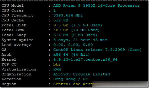
webhosting24:€28/年,日本NVMe3900X+Webvps
webhosting24决定从7月1日开始对日本机房的VPS进行NVMe和流量大升级,几乎是翻倍了硬盘和流量,当然前提是价格依旧不变。目前来看,国内过去走的是NTT直连,服务器托管机房应该是CDN77*(也就是datapacket.com),加上高性能平台(AMD Ryzen 9 3900X+NVMe),这样的日本VPS还是有相当大的性价比的。官方网站:https://www.webhosting...

SugarHosts糖果主机,(67元/年)云服务器/虚拟主机低至半价
SugarHosts 糖果主机商也算是比较老牌的主机商,从2009年开始推出虚拟主机以来,目前当然还是以虚拟主机为主,也有新增云服务器和独立服务器。早年很多网友也比较争议他们家是不是国人商家,其实这些不是特别重要,我们很多国人商家或者国外商家主要还是看重的是品质和服务。一晃十二年过去,有看到SugarHosts糖果主机商12周年的促销活动。如果我们有需要香港、美国、德国虚拟主机的可以选择,他们家的...

网站加v为你推荐
-
学员flashaccess数据库修复Access数据库恢复,有些表被损坏或有些表的部分记录被损坏,求解啊新iphone也将禁售iPhone8plus在2020年还会有货吗360arp防火墙在哪360ARP防火墙哪里下载?ipad代理想买个ipad,3000至4000元左右有什么好的开心001开心001与开心网怎么不一样,哪个是真的?大飞资讯新闻资讯包括什么内容?大飞资讯单仁资讯的黄功夫是何许人?温州商标注册温州代理注册个商标是怎么收费的?curl扩展大神帮忙看下centos 7.2 系统 php7.0.12的 curl 扩展怎么开启,谢谢啦