Signalwww.520bubu.com
www.520bubu.com 时间:2021-04-07 阅读:()
TPS59116www.
ti.
comSLUSA57–NOVEMBER2010CompleteDDR,DDR2andDDR3MemoryPowerSolutionSynchronousBuckController,3-ALDO,BufferedReferenceforEmbeddedComputingSystemsCheckforSamples:TPS591161FEATURESDESCRIPTIONTheTPS59116providesacompletepowersupplyfor2SynchronousBuckController(VDDQ)DDR/SSTL-2,DDR2/SSTL-18,andDDR3memory–Wide-InputVoltageRange:3.
0-Vto28-Vsystems.
Itintegratesasynchronousbuckcontroller–DCAPModewith100-nsLoadStepwitha3-Asink/sourcetrackinglinearregulatorandResponsebufferedlownoisereference.
TheTPS59116offersthelowesttotalsolutioncostinsystemswherespace–CurrentModeOptionSupportsCeramicisatapremium.
TheTPS59116synchronousOutputCapacitorscontrollerrunsfixed400-kHzpseudo-constant–SupportsSoft-OffinS4/S5StatesfrequencyPWMwithanadaptiveon-timecontrolthat–CurrentSensingfromRDS(on)orResistorcanbeconfiguredinD-CAPModeforeaseofuseandfastesttransientresponseorincurrentmodeto–2.
5-V(DDR),1.
8-V(DDR2),Adjustabletosupportceramicoutputcapacitors.
The3-A1.
5-V(DDR3)orOutputRange0.
75-Vtosink/sourceLDOmaintainsfasttransientresponse3.
0-Vonlyrequiring20-μF(2*10μF)ofceramicoutput–EquippedwithPowerGood,Overvoltagecapacitance.
Inaddition,theLDOsupplyinputisProtectionandUndervoltageProtectionavailableexternallytosignificantlyreducethetotalpowerlosses.
TheTPS59116supportsallofthe3-ALDO(VTT),BufferedReference(VREF)sleepstatecontrolsplacingVTTathigh-ZinS3–CapabletoSinkandSource3A(suspendtoRAM)anddischargingVDDQ,VTTand–LDOInputAvailabletoOptimizePowerVTTREF(soft-off)inS4/S5(suspendtodisk).
LossesTPS59116hasalloftheprotectionfeaturesincludingthermalshutdownandisofferedina24-pin4mm*–RequiresSmall20-μFCeramicOutput4mmQFNpackage.
Capacitor–BufferedLowNoise10-mAVREFOutputAPPLICATIONS–Accuracy±20mVforbothVREFandVTTDDR/DDR2/DDR3/LPDDR3MemoryPower–SupportsHigh-ZinS3andSoft-OffinS4/S5SuppliesinEmbeddedComputingSystem–ThermalShutdownSSTL-2SSTL-18andHSTLTermination1Pleasebeawarethatanimportantnoticeconcerningavailability,standardwarranty,anduseincriticalapplicationsofTexasInstrumentssemiconductorproductsanddisclaimerstheretoappearsattheendofthisdatasheet.
2D-CAPisatrademarkofTexasInstruments.
PRODUCTIONDATAinformationiscurrentasofpublicationdate.
Copyright2010,TexasInstrumentsIncorporatedProductsconformtospecificationsperthetermsoftheTexasInstrumentsstandardwarranty.
Productionprocessingdoesnotnecessarilyincludetestingofallparameters.
TPS59116SLUSA57–NOVEMBER2010www.
ti.
comThisintegratedcircuitcanbedamagedbyESD.
TexasInstrumentsrecommendsthatallintegratedcircuitsbehandledwithappropriateprecautions.
Failuretoobserveproperhandlingandinstallationprocedurescancausedamage.
ESDdamagecanrangefromsubtleperformancedegradationtocompletedevicefailure.
Precisionintegratedcircuitsmaybemoresusceptibletodamagebecauseverysmallparametricchangescouldcausethedevicenottomeetitspublishedspecifications.
ORDERINGINFORMATION(1)MINIMUMORDERABLEPARTOUTPUTTAPACKAGEPINSORDERNUMBERSUPPLYQUANTITYLargeTPS59116RGER3000tape-and-reelPlasticQuadFlatPack-40°Cto85°C24(QFN)SmallTPS59116RGET250tape-and-reel(1)AllpackagingoptionshaveCuNIPDAUlead/ballfinish.
ABSOLUTEMAXIMUMRATINGS(1)overoperatingfree-airtemperaturerangeunlessotherwisenotedTPS59116UNITSVBST-0.
3to36VBSTwrtLL-0.
3to6VINInputvoltagerangeVCS,MODE,S3,S5,VTTSNS,VDDQSNS,V5IN,VLDOIN,VDDQSET,-0.
3to6V5FILTPGND,VTTGND,CS_GND-0.
3to0.
3DRVH-1.
0to36VOUTOutputvoltagerangeLL-1.
0to30VCOMP,DRVL,PGOOD,VTT,VTTREF-0.
3to6TAOperatingambienttemperaturerange-40to85°CTstgStoragetemperature-55to150(1)Stressesbeyondthoselistedunder"absolutemaximumratings"maycausepermanentdamagetothedevice.
Thesearestressratingsonly,andfunctionaloperationofthedeviceattheseoranyotherconditionsbeyondthoseindicatedunder"recommendedoperatingconditions"isnotimplied.
Exposuretoabsolute-maximum-ratedconditionsforextendedperiodsmayaffectdevicereliability.
Allvoltagevaluesarewithrespecttothenetworkgroundterminalunlessotherwisenoted.
RECOMMENDEDOPERATINGCONDITIONSMINMAXUNITSupplyvoltageV5IN,V5FILT4.
755.
25VVBST,DRVH-0.
134LL-0.
628VLDOIN,VTT,VTTSNS,VDDQSNS-0.
13.
6VoltagerangeVVTTREF-0.
11.
8PGND,VTTGND,CS_GND-0.
10.
1S3,S5,MODE,VDDQSET,CS,COMP,PGOOD,-0.
15.
25DRVLOperatingfree-airtemperature,TA-4085°CDISSIPATIONRATINGSDERATINGFACTORABOVETA=TA4.
5V,PGOOD=HI91011ITRIPCurrentsensesinkcurrentμATA=25°C,VCS>4.
5V,PGOOD=LO456TRIPcurrenttemperatureRDS(on)sensescheme,OnthebasisTCITRIP4500ppm/°CcoefficientofTA=25°C(2)Overcurrentprotection(VV5IN-CS-VPGND-LL),VV5IN-CS=60mV,VOCL(off)-505COMPoffsetVCS>4.
5V(2)mVCurrentlimitthresholdsettingVR(trip)VV5IN-CS(2)30150rangePOWERGOODCOMPARATORPGinfromlower92.
5%95.
0%97.
5%VTVDDQPGVDDQpowergoodthresholdPGinfromhigher102.
5%105.
0%107.
5%PGhysteresis5%IPG(max)PGOODsinkcurrentVVTT=0V,VPGOOD=0.
5V2.
57.
5mAtPG(del)PGOODdelaytimeDelayforPGin80130200μsUNDERVOLTAGELOCKOUT/LOGICTHRESHOLDWakeup3.
74.
04.
3V5INUVLOthresholdVUVV5INvoltageHysteresis0.
20.
30.
4Nodischarge4.
7VTHMODEMODEthresholdNon-trackingdischarge0.
12.
5Voutput0.
080.
150.
25VVTHVDDQSETVDDQSETthresholdvoltage1.
8Voutput3.
54.
04.
5VIHHigh-levelinputvoltageS3,S52.
2VILLow-levelinputvoltageS3,S50.
3VIHYSTHysteresisvoltageS3,S50.
2VINLEAKLogicinputleakagecurrentS3,S5,MODE-11μAVINVDDQSETInputleakage/biascurrentVDDQSET-11(2)Ensuredbydesign.
Notproductiontested.
Copyright2010,TexasInstrumentsIncorporatedSubmitDocumentationFeedback5ProductFolderLink(s):TPS59116TPS59116SLUSA57–NOVEMBER2010www.
ti.
comELECTRICALCHARACTERISTICS(continued)overoperatingfree-airtemperaturerange,VV5IN=VV5FILT=5V,VLDOINisconnectedtoVDDQoutput(unlessotherwisenoted)PARAMETERTESTCONDITIONSMINTYPMAXUNITUNDERVOLTAGEANDOVERVOLTAGEPROTECTIONOVPdetect110%115%120%VDDQOVPtripthresholdVOVPvoltageHysteresis5%VDDQOVPpropagationTOVPDEL1.
5μsdelay(3)UVPdetect70%VUVPOutputUVPtripthresholdHysteresis10%OutputUVPpropagationtUVPDEL32delay(3)cycletUVPENOutputUVPenabledelay(3)1007THERMALSHUTDOWNShutdowntemperature160TSDNThermalSDNthreshold(3)°CHysteresis10(3)Ensuredbydesign.
Notproductiontested.
6SubmitDocumentationFeedbackCopyright2010,TexasInstrumentsIncorporatedProductFolderLink(s):TPS59116TPS59116www.
ti.
comSLUSA57–NOVEMBER2010DEVICEINFORMATIONTERMINALFUNCTIONSTERMINALI/ODESCRIPTIONNAMENO.
Outputofthetransconductanceamplifierforphasecompensation.
ConnecttoV5INtodisablegmCOMP6I/OamplifieranduseD-CAPmode.
Currentsensecomparatorinput(-)forresistorcurrentsensescheme.
OrovercurrenttripvoltageCS16I/OsettinginputforRDS(on)currentsenseschemeifconnectedtoV5FILTthroughthevoltagesettingresistor.
DRVH21OSwitching(top)MOSFETgatedriveoutput.
DRVL19ORectifying(bottom)MOSFETgatedriveoutput.
GND3-Signalground.
ConnecttominusterminaloftheVTTLDOoutputcapacitor.
CS_GND17Currentsensecomparatorinput(+)andgroundforpowergoodcircuit.
Switching(top)MOSFETgatedriverreturn.
Currentsensecomparatorinput(-)forRDS(on)currentLL20I/Osense.
MODE4IDischargemodesettingpin.
SeeVDDQandVTTDischargeControlsection.
NC7,12Noconnect.
PGND18-Groundforrectifying(bottom)MOSFETgatedriver.
Powergoodsignalopendrainoutput,InHIGHstatewhenVDDQoutputvoltageiswithinthetargetPGOOD13Orange.
S310IS3signalinput.
S511IS5signalinput.
V5IN15I5-VpowersupplyinputforMOSFETgatedrivers.
V5FILT14IFiltered5-Vpowersupplyinputforinternalcircuits.
ConnectR-CnetworkfromV5INtoV5FILT.
VBST22I/OSwitching(top)MOSFETdriverbootstrapvoltageinput.
VDDQSET9IVDDQoutputvoltagesettingpin.
SeeVDDQOutputVoltageSelectionsection.
VDDQreferenceinputforVTTandVTTREF.
PowersupplyfortheVTTREF.
DischargecurrentVDDQSNS8I/OsinkingterminalforVDDQNon-trackingdischarge.
OutputvoltagefeedbackinputforVDDQoutputifVDDQSETpinisconnectedtoV5INorGND.
VLDOIN23IPowersupplyfortheVTTLDO.
VTT24OPoweroutputfortheVTTLDO.
VTTGND1-PowergroundoutputfortheVTTLDO.
VTTREF5OVTTREFbufferedreferenceoutput.
VTTSNS2IVoltagesenseinputfortheVTTLDO.
ConnecttoplusterminaloftheVTTLDOoutputcapacitor.
Copyright2010,TexasInstrumentsIncorporatedSubmitDocumentationFeedback7ProductFolderLink(s):TPS59116TPS59116SLUSA57–NOVEMBER2010www.
ti.
comFUNCTIONALBLOCKDIAGRAM(RGE)8SubmitDocumentationFeedbackCopyright2010,TexasInstrumentsIncorporatedProductFolderLink(s):TPS59116TPS59116www.
ti.
comSLUSA57–NOVEMBER2010DETAILEDDESCRIPTIONTheTPS59116isanintegratedpowermanagementsolutionwhichcombinesasynchronousbuckcontroller,a10-mAbufferedreferenceandahigh-currentsink/sourcelow-dropoutlinearregulator(LDO)inasmall20-pinHTSSOPpackageora24-pinQFNpackage.
EachoftheserailsgeneratesVDDQ,VTTREFandVTTthatrequiredwithDDR/DDR2/DDR3memorysystems.
Theswitchmodepowersupply(SMPS)portionemploysexternalN-channelMOSFETstosupporthighcurrentforDDR/DDR2/DDR3memory'sVDD/VDDQ.
Thepresetoutputvoltageisselectablefrom2.
5Vor1.
8V.
Userdefinedoutputvoltageisalsopossibleandcanbeadjustablefrom0.
75Vto3V.
InputvoltagerangeoftheSMPSis3Vto28V.
TheSMPSrunsanadaptiveon-timePWMoperationathigh-loadconditionandautomaticallyreducesfrequencytokeepexcellentefficiencydowntoseveralmA.
CurrentsensingschemeuseseitherRDS(on)oftheexternalrectifyingMOSFETforalow-cost,loss-lesssolution,oranoptionalsenseresistorplacedinseriestotherectifyingMOSFETformoreaccuratecurrentlimit.
TheoutputoftheswitcherissensedbyVDDQSNSpintogenerateone-halfVDDQforthe10-mAbufferedreference(VTTREF)andtheVTTactiveterminationsupply.
TheVTTLDOcansourceandsinkupto3-Apeakcurrentwithonly20-μF(two10-μFinparallel)ceramicoutputcapacitors.
VTTREFtracksVDDQ/2within±1%ofVDDQ.
VTToutputtracksVTTREFwithin±20mVatnoloadconditionwhile±40mVatfullload.
TheLDOinputcanbeseparatedfromVDDQandoptionallyconnectedtoalowervoltagebyusingVLDOINpin.
Thishelpsreducingpowerdissipationinsourcingphase.
TheTPS59116isfullycompatibletoJEDECDDR/DDR2specificationsatS3/S5sleepstate(seeTable2).
TheparthastwooptionsofoutputdischargefunctionwhenbothVTTandVDDQaredisabled.
ThetrackingdischargemodedischargesVDDQandVTToutputsthroughtheinternalLDOtransistorsandthenVTToutputtrackshalfofVDDQvoltageduringdischarge.
Thenon-trackingdischargemodedischargesoutputsusinginternaldischargeMOSFETswhichareconnectedtoVDDQSNSandVTT.
ThecurrentcapabilityofthesedischargeFETsarelimitedanddischargeoccursmoreslowlythanthetrackingdischarge.
Thesedischargefunctionscanbedisabledbyselectingnon-dischargemode.
VDDQSMPS,DualPWMOperationModesThemaincontrolloopoftheSMPSisdesignedasanadaptiveon-timepulsewidthmodulation(PWM)controller.
ItsupportstwocontrolschemeswhichareacurrentmodeandaproprietaryD-CAPmode.
D-CAPmodeusesinternalcompensationcircuitandissuitableforlowexternalcomponentcountconfigurationwithanappropriateamountofESRattheoutputcapacitor(s).
Currentmodecontrolhasmoreflexibility,usingexternalcompensationnetwork,andcanbeusedtoachievestableoperationwithverylowESRcapacitor(s)suchasceramicorspecialtypolymercapacitors.
ThesecontrolmodesareselectedbytheCOMPterminalconnection.
IftheCOMPpinisconnectedtoV5IN,TPS59116worksintheD-CAPmode,otherwiseitworksinthecurrentmode.
VDDQoutputvoltageismonitoredatafeedbackpointvoltage.
IfVDDQSETisconnectedtoV5INorGND,thisfeedbackpointistheoutputoftheinternalresistordividerinsideVDDQSNSpin.
IfanexternalresistordividerisconnectedtoVDDQSETpin,VDDQSETpinitselfbecomesthefeedbackpoint(seeVDDQOutputVoltageSelectionsection).
Atthebeginningofeachcycle,thesynchronoustopMOSFETisturnedon,orbecomesONstate.
ThisMOSFETisturnedoff,orbecomesOFFstate,afterinternaloneshottimerexpires.
ThisoneshotisdeterminedbyVINandVOUTtokeepfrequencyfairlyconstantoverinputvoltagerange,henceitiscalledadaptiveon-timecontrol(seePWMFrequencyandAdaptiveOn-TimeControlsection).
TheMOSFETisturnedonagainwhenfeedbackinformationindicatesinsufficientoutputvoltageandinductorcurrentinformationindicatesbelowtheovercurrentlimit.
Repeatingoperationinthismanner,thecontrollerregulatestheoutputvoltage.
ThesynchronousbottomortherectifyingMOSFETisturnedoneachOFFstatetokeeptheconductionlossminimum.
TherectifyingMOSFETisturnedoffwheninductorcurrentinformationdetectszerolevel.
Thisenablesseamlesstransitiontothereducedfrequencyoperationatlightloadconditionsothathighefficiencyiskeptoverbroadrangeofloadcurrent.
Inthecurrentmodecontrolscheme,thetransconductanceamplifiergeneratesatargetcurrentlevelcorrespondingtothevoltagedifferencebetweenthefeedbackpointandtheinternal750mVreference.
DuringtheOFFstate,thePWMcomparatormonitorstheinductorcurrentsignalaswellasthistargetcurrentlevel,andwhentheinductorcurrentsignalcomeslowerthanthetargetcurrentlevel,thecomparatorprovidesSETsignaltoinitiatethenextONstate.
ThevoltagefeedbackgainisadjustableoutsidethecontrollerdevicetosupportvarioustypesofoutputMOSFETsandcapacitors.
IntheD-CAPmode,thetransconductanceamplifierisdisabledandthePWMcomparatorcomparesthefeedbackpointvoltageandtheinternal750mVreferenceduringtheOFFstate.
Whenthefeedbackpointcomeslowerthanthereferencevoltage,thecomparatorprovidesSETsignaltoinitiatethenextONstate.
Copyright2010,TexasInstrumentsIncorporatedSubmitDocumentationFeedback9ProductFolderLink(s):TPS59116TPS59116SLUSA57–NOVEMBER2010www.
ti.
comVDDQSMPS,LightLoadConditionTPS59116automaticallyreducesswitchingfrequencyatlightloadconditiontomaintainhighefficiency.
ThisreductionoffrequencyisachievedsmoothlyandwithoutincreaseofVOUTrippleorloadregulation.
Detailoperationisdescribedasfollows.
Astheoutputcurrentdecreasesfromheavyloadcondition,theinductorcurrentisalsoreducedandeventuallycomestothepointthatitsvalleytoucheszerocurrent,whichistheboundarybetweencontinuousconductionanddiscontinuousconductionmodes.
TherectifyingMOSFETisturnedoffwhenthiszeroinductorcurrentisdetected.
Astheloadcurrentfurtherdecreased,theconverterrunsindiscontinuousconductionmodeandittakeslongerandlongertodischargetheoutputcapacitortothelevelthatrequiresnextONcycle.
TheON-timeiskeptthesameasthatintheheavyloadcondition.
Inreverse,whentheoutputcurrentincreasefromlightloadtoheavyload,switchingfrequencyincreasestotheconstant400kHzastheinductorcurrentreachestothecontinuousconduction.
ThetransitionloadpointtothelightloadoperationIOUT(LL)(i.
e.
thethresholdbetweencontinuousanddiscontinuousconductionmode)canbecalculatedinEquation1:wherefisthePWMswitchingfrequency(400kHz)(1)SwitchingfrequencyversusoutputcurrentinthelightloadconditionisafunctionofL,f,VINandVOUT,butitdecreasesalmostproportionaltotheoutputcurrentfromtheIOUT(LL)givenabove.
Forexample,itis40kHzatIOUT(LL)/10and4kHzatIOUT(LL)/100.
Low-SideDriverThelow-sidedriverisdesignedtodrivehigh-current,low-RDS(on),N-channelMOSFET(s).
Thedrivecapabilityisrepresentedbyitsinternalresistance,whichare3forV5INtoDRVLand0.
9forDRVLtoPGND.
Adead-timetopreventshootthroughisinternallygeneratedbetweentopMOSFETofftobottomMOSFETon,andbottomMOSFETofftotopMOSFETon.
5-VbiasvoltageisdeliveredfromV5INsupply.
TheinstantaneousdrivecurrentissuppliedbyaninputcapacitorconnectedbetweenV5INandGND.
TheaveragedrivecurrentisequaltothegatechargeatVGS=5Vtimesswitchingfrequency.
Thisgatedrivecurrentaswellasthehigh-sidegatedrivecurrenttimes5VmakesthedrivingpowerwhichneedstobedissipatedfromTPS59116package.
High-SideDriverThehigh-sidedriverisdesignedtodrivehigh-current,low-RDS(on)N-channelMOSFET(s).
Whenconfiguredasafloatingdriver,5-VbiasvoltageisdeliveredfromV5INsupply.
TheaveragedrivecurrentisalsocalculatedbythegatechargeatVGS=5Vtimesswitchingfrequency.
TheinstantaneousdrivecurrentissuppliedbytheflyingcapacitorbetweenVBSTandLLpins.
Thedrivecapabilityisrepresentedbyitsinternalresistance,whichare3forVBSTtoDRVHand0.
9forDRVHtoLL.
CurrentSensingSchemeInordertoprovidebothgoodaccuracyandcosteffectivesolution,TPS59116supportsbothofexternalresistorsensingandMOSFETRDS(on)sensing.
Forresistorsensingscheme,anappropriatecurrentsensingresistorshouldbeconnectedbetweenthesourceterminalofthebottomMOSFETandPGND.
CSpinisconnectedtotheMOSFETsourceterminalnode.
TheinductorcurrentismonitoredbythevoltagebetweenPGNDpinandCSpin.
ForRDS(on)sensingscheme,CSpinshouldbeconnectedtoV5FILTthroughthetripvoltagesettingresistor,RTRIP.
Inthisscheme,CSterminalsinks10-μAITRIPcurrentandthetriplevelissettothevoltageacrosstheRTRIP.
TheinductorcurrentismonitoredbythevoltagebetweenPGNDpinandLLpinsothatLLpinshouldbeconnectedtothedrainterminalofthebottomMOSFET.
ITRIPhas4500ppm/°CtemperatureslopetocompensatethetemperaturedependencyoftheRDS(on).
Ineitherscheme,PGNDisusedasthepositivecurrentsensingnodesothatPGNDshouldbeconnectedtothepropercurrentsensingdevice,i.
e.
thesenseresistororthesourceterminalofthebottomMOSFET.
10SubmitDocumentationFeedbackCopyright2010,TexasInstrumentsIncorporatedProductFolderLink(s):TPS59116TPS59116www.
ti.
comSLUSA57–NOVEMBER2010PWMFrequencyandAdaptiveOn-TimeControlTPS59116employsadaptiveon-timecontrolschemeanddoesnothaveadedicatedoscillatoronboard.
However,thedevicerunswithfixed400-kHzpseudo-constantfrequencybyfeed-forwardingtheinputandoutputvoltageintotheon-timeone-shottimer.
Theon-timeiscontrolledinverseproportionaltotheinputvoltageandproportionaltotheoutputvoltagesothatthedutyratioiskeptasVOUT/VINtechnicallywiththesamecycletime.
AlthoughtheTPS59116doesnothaveapinconnectedtoVIN,theinputvoltageismonitoredatLLpinduringtheONstate.
Thishelpspincountreductiontomakethepartcompactwithoutsacrificingitsperformance.
InordertosecureminimumON-timeduringstartup,feed-forwardfromtheoutputvoltageisenabledaftertheoutputbecomes750mVorlarger.
VDDQOutputVoltageSelectionTPS59116canbeusedforbothofDDR(VVDDQ=2.
5V)andDDR2(VVDDQ=1.
8V)powersupplyandadjustableoutputvoltage(0.
75V>ESR,RO>>RCandCC>>CC2,eachtransferfunctionofthethreeblocksisshownstartingwithEquation7.
(7)(8)(9)TherearethreepolesandtwozerosinH(s).
Eachpoleandzeroisgivenbythefollowingfiveequations.
(10)(11)Copyright2010,TexasInstrumentsIncorporatedSubmitDocumentationFeedback15ProductFolderLink(s):TPS59116TPS59116SLUSA57–NOVEMBER2010www.
ti.
com(12)(13)(14)Usually,eachfrequencyofthosepolesandzerosislowerthanthe0dBfrequency,f0.
However,thef0shouldbekeptunder1/3oftheswitchingfrequencytoavoideffectofswitchingcircuitdelay.
Thef0isgivenbyEquation15.
(15)Basedonsmallsignalanalysisabove,theexternalcomponentscanbeselectedbyfollowingmanner.
1.
Choosetheinductor.
Theinductancevalueshouldbedeterminedtogivetheripplecurrentofapproximately1/4to1/2ofmaximumoutputcurrent.
(16)TheinductoralsoneedstohavelowDCRtoachievegoodefficiency,aswellasenoughroomabovepeakinductorcurrentbeforesaturation.
ThepeakinductorcurrentcanbeestimatedasshowninEquation17.
(17)2.
Chooserectifying(bottom)MOSFET.
WhenRDS(on)sensingschemeisselected,therectifyingMOSFET'son-resistanceisusedasthisRSsothatlowerRDS(on)doesnotalwayspromisebetterperformance.
Inordertoclearlydetectinductorcurrent,minimumRSrecommendedistogive15mVorlargerripplevoltagewiththeinductorripplecurrent.
ThispromisessmoothtransitionfromCCMtoDCMorviceversa.
UppersideoftheRDS(on)isofcourserestrictedbytheefficiencyrequirement,andusuallythisresistanceaffectsefficiencymoreathigh-loadconditions.
Whenusingexternalresistorcurrentsensing,thereisnorestrictionforlowRDS(on).
However,thecurrentsensingresistanceRSitselfaffectstheefficiency3.
Chooseoutputcapacitor(s).
Incasesoforganicsemiconductorcapacitors(OS-CON)orspecialtypolymercapacitors(SP-CAP),ESRtoachieverequiredripplevalueatstablestateortransientloadconditionsdeterminestheamountofcapacitor(s)need,andcapacitanceisthenenoughtosatisfystableoperation.
Thepeak-to-peakripplevaluecanbeestimatedbyESRtimestheinductorripplecurrentforstablestate,orESRtimestheloadcurrentstepforafasttransientloadresponse.
Incaseofceramiccapacitor(s),usuallyESRissmallenoughtomeetripplerequirement.
Ontheotherhand,transientundershootandovershootdrivenbyoutputcapacitancebecomesthekeyfactortodeterminethecapacitor(s).
4.
Determinef0andcalculateRCusingEquation18.
NotethathigherRCshowsfastertransientresponseincostofunstableness.
IfthetransientresponseisnotenoughevenwithhighRCvalue,tryincreasingtheoutputcapacitance.
Recommendedf0isfOSC/4.
ThenRCcanbederivedbyEquation19.
(18)(19)5.
CalculateCC2.
ThiscapacitancecancelsthezerocausedbyESRoftheoutputcapacitor.
Whenusingceramiccapacitor(s),thereisnoneedforCC2.
(20)(21)16SubmitDocumentationFeedbackCopyright2010,TexasInstrumentsIncorporatedProductFolderLink(s):TPS59116TPS59116www.
ti.
comSLUSA57–NOVEMBER20106.
CalculateCC.
ThepurposeofCCistoreducetheDCcomponenttoobtainhighDCfeedbackgain.
However,asitcausesphasedelay,anotherzeroisneededtocancelthiseffect.
Thiszero,ωz1,isdeterminedbyCCandRC.
Itisrecommendedthatωz1be10timeslowerthanthef0frequency.
(22)7.
Whenusingadjustablemode,determinethevalueofR1andR2.
.
(23)D-CAPModeOperationAbuckconvertersystemusingD-CAPModecanbesimplifiedasbelow.
Figure3.
LinearizingtheModulatorTheVDDQSNSvoltageiscomparedtotheinternalreferencevoltageafterdividerresistors.
ThePWMcomparatordeterminesthetimetoturn-onthetopMOSFET.
Thegainandspeedofthecomparatorishighenoughtokeepthevoltageatthebeginningofeachoncycle(ortheendofeachoffcycle)substantiallyconstant.
TheDCoutputvoltagemayhavelineregulationduetorippleamplitudethatslightlyincreasesastheinputvoltageincrease.
Forloopstability,the0-dBfrequency,f0,definedinEquation24needstobelowerthan1/3oftheswitchingfrequency.
(24)Asf0isdeterminedsolelybytheoutputcapacitorcharacteristics,loopstabilityofD-CAPmodeisdeterminedbythecapacitorchemistry.
Forexample,specialtypolymercapacitors(SP-CAP)haveCOintheorderofseveral100μFandhaveanESRintherangeof10m.
Thismakesf0ontheorderof100kHzorlessandtheloopisthenstable.
However,ceramiccapacitorshaveanf0ofmorethan700kHz,whichisnotsuitableforthisoperationalmode.
AlthoughD-CAPmodeprovidesmanyadvantagessuchasease-of-use,minimumexternalcomponentsconfigurationandextremelyshortresponsetime,becausethereisnoerroramplifierintheloop,asufficientamountoffeedbacksignalneedstobeprovidedbyanexternalcircuittoreducejitterlevel.
Therequiredsignallevelisapproximately15mVatthecomparingpoint.
ThisgivesVRIPPLE=(VOUT/0.
75)x15(mV)attheoutputnode.
TheoutputcapacitorESRshouldmeetthisrequirement.
Copyright2010,TexasInstrumentsIncorporatedSubmitDocumentationFeedback17ProductFolderLink(s):TPS59116TPS59116SLUSA57–NOVEMBER2010www.
ti.
comTheexternalcomponentsselectionismuchmoresimpleinD-CAPmode.
1.
Chooseinductor.
Thissectionisthesameasthecurrentmode.
PleaserefertotheinstructionsintheCurrentModeOperationsection.
2.
Chooseoutputcapacitor(s).
Organicsemiconductorcapacitor(s)orspecialtypolymercapacitor(s)arerecommended.
DetermineanESRtomeettherequiredripplevoltage.
AquickapproximationisshowninEquation25.
(25)ThermalDesignPrimarypowerdissipationoftheTPS59116isgeneratedfromtheVTTregulator.
TheVTTcurrentflowinbothsourceandsinkdirectionsgeneratespowerdissipationfromthedevice.
Inthesourcephase,thepotentialdifferencebetweenVLDOINandVTTtimesVTTcurrentbecomesthepowerdissipation,WDSRC.
(26)Inthiscase,ifVLDOINisconnectedtoanalternativepowersupplylowerthanVDDQvoltage,powerlosscanbedecreased.
Forthesinkphase,VTTvoltageisappliedacrosstheinternalLDOregulator,andthepowerdissipation,WDSNK,iscalculatedbyEquation27:(27)BecausethisdevicedoesnotsinkANDsourcethecurrentatthesametimeandIVTTvariesrapidlywithtime,theactualpowerdissipationthatmustbeconsideredforthermaldesignisanaverageofWDSNK.
AnotherpowerconsumptionisthecurrentusedforinternalcontrolcircuitryfromV5INsupplyandVLDOINsupply.
V5INsupportsboththeinternalcircuitandexternalMOSFETsdrivecurrent.
TheformercurrentisintheVLDOINsupplycanbeestimatedas1.
5mAorlessatnormaloperationalconditions.
Thesepowersneedtobeeffectivelydissipatedfromthepackage.
MaximumpowerdissipationallowedtothepackageiscalculatedbyEquation28,where(28)TJ(max)is125°CTA(max)isthemaximumambienttemperatureinthesystemθJAisthethermalresistancefromthesiliconjunctiontotheambient18SubmitDocumentationFeedbackCopyright2010,TexasInstrumentsIncorporatedProductFolderLink(s):TPS59116TPS59116www.
ti.
comSLUSA57–NOVEMBER2010Thisthermalresistancestronglydependsontheboardlayout.
TPS59116isassembledinathermallyenhancedPowerPADpackagethathasexposeddiepadunderneaththebody.
Forimprovedthermalperformance,thisdiepadneedstobeattachedtogroundtraceviathermallandonthePCB.
Thisgroundtraceactsasaheatsink/spread.
Thetypicalthermalresistance,39.
6°C/W,isachievedbasedona6.
5mm*3.
4mmthermallandwitheightviaswithoutairflow.
Itcanbeimprovedbyusinglargerthermallandand/orincreasingviasnumber.
FurtherinformationaboutPowerPADanditsrecommendedboardlayoutisdescribedin(SLMA002).
Thisdocumentisavailableathttp:\\www.
ti.
com.
LayoutConsiderationsCertainpointsmustbeconsideredbeforedesigningalayoutusingtheTPS59116.
ThePCBtraceisdefinedasLLnode,whichconnectstothesourceoftheswitchingMOSFET,thedrainoftherectifyingMOSFETandthehigh-voltagesideoftheinductor,shouldbeasshortandwideaspossible.
Consideraddingasmallsnubbercircuit,consistingof3and1nF,betweenLLandPGNDincaseahigh-frequencyringingisobservedontheLLvoltagewaveform.
AllsensitiveanalogtracessuchasVDDQSNS,VTTSNSandCSshouldbeplacedawayfromhigh-voltageswitchingnodessuchasLL,DRVLorDRVHnodestoavoidcoupling.
VLDOINshouldbeconnectedtoVDDQoutputwithashortandwidetrace.
IfadifferentpowersourceisusedforVLDOIN,aninputbypasscapacitorshouldbeplacedtothepinascloseaspossiblewithashortandwideconnection.
TheoutputcapacitorforVTTshouldbeplacedascloseaspossibletothepinwithashortandwideconnectioninordertoavoidadditionalESRand/orESLofthetrace.
VTTSNSshouldbeconnectedtothepositivenodeofVTToutputcapacitor(s)asaseparatetracefromthehigh-currentpowerlineandisstronglyrecommendedtoavoidadditionalESRand/orESL.
Ifitisneededtosensethevoltageofthepointoftheload,itisrecommendedtoattachtheoutputcapacitor(s)atthatpoint.
Also,itisrecommendedtominimizeanyadditionalESRand/orESLofgroundtracebetweenGNDpinandtheoutputcapacitor(s).
ConsideraddingLPFatVTTSNSincaseESRoftheVTToutputcapacitor(s)islargerthan2m.
VDDQSNScanbeconnectedseparatelyfromVLDOIN.
RememberthatthissensingpotentialisthereferencevoltageofVTTREF.
Avoidanynoisegenerativelines.
NegativenodeofVTToutputcapacitor(s)andVTTREFcapacitorshouldbetiedtogetherbyavoidingcommonimpedancetothehighcurrentpathoftheVTTsource/sinkcurrent.
GND(SignalGND)pinnoderepresentsthereferencepotentialforVTTREFandVTToutputs.
ConnectGNDtonegativenodesofVTTcapacitor(s),VTTREFcapacitorandVDDQcapacitor(s)withcaretoavoidadditionalESRand/orESL.
GNDandPGND(powerground)shouldbeconnectedtogetheratasinglepoint.
ConnectCS_GND(RGE)tosourceofrectifyingMOSFETusingKevinconnection.
Avoidcommontraceforhigh-currentpathssuchastheMOSFETtotheoutputcapacitorsorthePGNDtotheMOSFETtrace.
Incaseofusingexternalcurrentsenseresistor,applythesamecareandconnectittothepositiveside(groundside)oftheresistor.
PGNDisthereturnpathforrectifyingMOSFETgatedrive.
Use0.
65mm(25mil)orwidertrace.
ConnecttosourceofrectifyingMOSFETwithshortestpossiblepath.
PlaceaV5FILTfiltercapacitor(RGE)closetotheTPS59116,within12mm(0.
5inches)ifpossible.
ThetracefromtheCSpinshouldavoidhigh-voltageswitchingnodessuchasthoseforLL,VBST,DRVH,DRVLorPGOOD.
Inordertoeffectivelyremoveheatfromthepackage,preparethermallandandsoldertothepackage'sthermalpad.
Widetraceofthecomponent-sidecopper,connectedtothisthermalland,helpsheatspreading.
Numerousviaswitha0.
33-mmdiameterconnectedfromthethermallandtotheinternal/solder-sidegroundplane(s)shouldbeusedtohelpdissipation.
DoNOTconnectPGNDtothisthermallandpadunderneaththepackage.
Copyright2010,TexasInstrumentsIncorporatedSubmitDocumentationFeedback19ProductFolderLink(s):TPS59116TPS59116SLUSA57–NOVEMBER2010www.
ti.
comFigure4.
D-CAPModeTable4.
D-CAPModeSchematicComponentsSYMBOLSPECIFICATIONMANUFACTURERPARTNUMBERR15.
1k-R2100k-R375k-R4(100*VVDDQ–75)k-R55.
1M130V,13mInternationalRectifierIRF7821M230V,5mInternationalRectifierIRF783220SubmitDocumentationFeedbackCopyright2010,TexasInstrumentsIncorporatedProductFolderLink(s):TPS59116TPS59116www.
ti.
comSLUSA57–NOVEMBER2010Figure5.
CurrentModeTable5.
CurrentModeSchematicComponentsSYMBOLSPECIFICATIONMANUFACTURERPARTNUMBERR16m,1%VishayWSL-25210.
006R2100k--R55.
1M030V,13mInternationalRectifierIRF7821M130V,5mInternationalRectifierIRF7832Copyright2010,TexasInstrumentsIncorporatedSubmitDocumentationFeedback21ProductFolderLink(s):TPS59116TPS59116SLUSA57–NOVEMBER2010www.
ti.
comTYPICALCHARACTERISTICSV5IN+V5FILTSUPPLYCURRENTV5IN+V5FILTSHUTDOWNCURRENTvsvsJUNCTIONTEMPERATUREJUNCTIONTEMPERATUREFigure6.
Figure7.
V5IN+V5FILTSUPPLYCURRENTVLDOINSUPPLYCURRENTvsvsLOADCURRENTTEMPERATUREFigure8.
Figure9.
22SubmitDocumentationFeedbackCopyright2010,TexasInstrumentsIncorporatedProductFolderLink(s):TPS59116TPS59116www.
ti.
comSLUSA57–NOVEMBER2010TYPICALCHARACTERISTICS(continued)CSCURRENTVDDQDISCHARGECURRENTvsvsJUNCTIONTEMPERATUREJUNCTIONTEMPERATUREFigure10.
Figure11.
VTTDISCHARGECURRENTOVERVOLTAGEANDUNDERVOLTAGETHRESHOLDvsvsJUNCTIONTEMPERATUREJUNCTIONTEMPERATUREFigure12.
Figure13.
Copyright2010,TexasInstrumentsIncorporatedSubmitDocumentationFeedback23ProductFolderLink(s):TPS59116TPS59116SLUSA57–NOVEMBER2010www.
ti.
comTYPICALCHARACTERISTICS(continued)SWITCHINGFREQUENCYSWITCHINGFREQUENCYvsvsINPUTVOLTAGEOUTPUTCURRENTFigure14.
Figure15.
VDDQOUTPUTVOLTAGEVDDQOUTPUTVOLTAGEvsvsOUTPUTCURRENT(DDR)INPUTVOLTAGE(DDR2)Figure16.
Figure17.
24SubmitDocumentationFeedbackCopyright2010,TexasInstrumentsIncorporatedProductFolderLink(s):TPS59116TPS59116www.
ti.
comSLUSA57–NOVEMBER2010TYPICALCHARACTERISTICS(continued)VTTOUTPUTVOLTAGEVTTOUTPUTVOLTAGEvsvsOUTPUTCURRENT(DDR)OUTPUTCURRENT(DDR2)Figure18.
Figure19.
VTTREFOUTPUTVOLTAGEVTTREFOUTPUTVOLTAGEvsvsOUTPUTCURRENT(DDR)OUTPUTCURRENT(DDR2)Figure20.
Figure21.
Copyright2010,TexasInstrumentsIncorporatedSubmitDocumentationFeedback25ProductFolderLink(s):TPS59116TPS59116SLUSA57–NOVEMBER2010www.
ti.
comTYPICALCHARACTERISTICS(continued)VTTREFOUTPUTVOLTAGEVTTOUTPUTVOLTAGEvsvsOUTPUTCURRENT(DDR3)OUTPUTCURRENT(DDR3)Figure22.
Figure23.
VDDQEFFICIENCY(DDR)VDDQEFFICIENCY(DDR2)vsvsVDDQCURRENTVDDQCURRENTFigure24.
Figure25.
26SubmitDocumentationFeedbackCopyright2010,TexasInstrumentsIncorporatedProductFolderLink(s):TPS59116TPS59116www.
ti.
comSLUSA57–NOVEMBER2010TYPICALCHARACTERISTICS(continued)Figure26.
RippleWaveforms-HeavyLoadConditionFigure27.
VDDQLoadTransientResponseFigure28.
VTTLoadTransientResponseFigure29.
VDDQ,VTT,andVTTREFStart-UpWaveformsCopyright2010,TexasInstrumentsIncorporatedSubmitDocumentationFeedback27ProductFolderLink(s):TPS59116TPS59116SLUSA57–NOVEMBER2010www.
ti.
comTYPICALCHARACTERISTICS(continued)Figure30.
Soft-StartWaveformsTrackingDischargeFigure31.
Pre-BiasedStart-Up:VDDQ,VTT,andPGOODVDDQBODEPLOT(CURRENTMODE)GAINANDPHASEvsFREQUENCYFigure32.
Soft-StopWaveformsNon-TrackingDischargeFigure33.
28SubmitDocumentationFeedbackCopyright2010,TexasInstrumentsIncorporatedProductFolderLink(s):TPS59116TPS59116www.
ti.
comSLUSA57–NOVEMBER2010TYPICALCHARACTERISTICS(continued)VTTBODEPLOT,SOURCE(DDR2)VTTBODEPLOT,SINK(DDR2)GAINANDPHASEGAINANDPHASEvsvsFREQUENCYFREQUENCYFigure34.
Figure35.
Copyright2010,TexasInstrumentsIncorporatedSubmitDocumentationFeedback29ProductFolderLink(s):TPS59116PACKAGEOPTIONADDENDUMwww.
ti.
com11-Apr-2013Addendum-Page1PACKAGINGINFORMATIONOrderableDeviceStatus(1)PackageTypePackageDrawingPinsPackageQtyEcoPlan(2)Lead/BallFinishMSLPeakTemp(3)OpTemp(°C)Top-SideMarkings(4)SamplesTPS59116RGERACTIVEVQFNRGE243000Green(RoHS&noSb/Br)CUNIPDAULevel-2-260C-1YEAR-40to85TPS59116TPS59116RGETACTIVEVQFNRGE24250Green(RoHS&noSb/Br)CUNIPDAULevel-2-260C-1YEAR-40to85TPS59116(1)Themarketingstatusvaluesaredefinedasfollows:ACTIVE:Productdevicerecommendedfornewdesigns.
LIFEBUY:TIhasannouncedthatthedevicewillbediscontinued,andalifetime-buyperiodisineffect.
NRND:Notrecommendedfornewdesigns.
Deviceisinproductiontosupportexistingcustomers,butTIdoesnotrecommendusingthispartinanewdesign.
PREVIEW:Devicehasbeenannouncedbutisnotinproduction.
Samplesmayormaynotbeavailable.
OBSOLETE:TIhasdiscontinuedtheproductionofthedevice.
(2)EcoPlan-Theplannedeco-friendlyclassification:Pb-Free(RoHS),Pb-Free(RoHSExempt),orGreen(RoHS&noSb/Br)-pleasecheckhttp://www.
ti.
com/productcontentforthelatestavailabilityinformationandadditionalproductcontentdetails.
TBD:ThePb-Free/Greenconversionplanhasnotbeendefined.
Pb-Free(RoHS):TI'sterms"Lead-Free"or"Pb-Free"meansemiconductorproductsthatarecompatiblewiththecurrentRoHSrequirementsforall6substances,includingtherequirementthatleadnotexceed0.
1%byweightinhomogeneousmaterials.
Wheredesignedtobesolderedathightemperatures,TIPb-Freeproductsaresuitableforuseinspecifiedlead-freeprocesses.
Pb-Free(RoHSExempt):ThiscomponenthasaRoHSexemptionforeither1)lead-basedflip-chipsolderbumpsusedbetweenthedieandpackage,or2)lead-baseddieadhesiveusedbetweenthedieandleadframe.
ThecomponentisotherwiseconsideredPb-Free(RoHScompatible)asdefinedabove.
Green(RoHS&noSb/Br):TIdefines"Green"tomeanPb-Free(RoHScompatible),andfreeofBromine(Br)andAntimony(Sb)basedflameretardants(BrorSbdonotexceed0.
1%byweightinhomogeneousmaterial)(3)MSL,PeakTemp.
--TheMoistureSensitivityLevelratingaccordingtotheJEDECindustrystandardclassifications,andpeaksoldertemperature.
(4)MultipleTop-SideMarkingswillbeinsideparentheses.
OnlyoneTop-SideMarkingcontainedinparenthesesandseparatedbya"~"willappearonadevice.
IfalineisindentedthenitisacontinuationofthepreviouslineandthetwocombinedrepresenttheentireTop-SideMarkingforthatdevice.
ImportantInformationandDisclaimer:TheinformationprovidedonthispagerepresentsTI'sknowledgeandbeliefasofthedatethatitisprovided.
TIbasesitsknowledgeandbeliefoninformationprovidedbythirdparties,andmakesnorepresentationorwarrantyastotheaccuracyofsuchinformation.
Effortsareunderwaytobetterintegrateinformationfromthirdparties.
TIhastakenandcontinuestotakereasonablestepstoproviderepresentativeandaccurateinformationbutmaynothaveconducteddestructivetestingorchemicalanalysisonincomingmaterialsandchemicals.
TIandTIsuppliersconsidercertaininformationtobeproprietary,andthusCASnumbersandotherlimitedinformationmaynotbeavailableforrelease.
InnoeventshallTI'sliabilityarisingoutofsuchinformationexceedthetotalpurchasepriceoftheTIpart(s)atissueinthisdocumentsoldbyTItoCustomeronanannualbasis.
TAPEANDREELINFORMATION*AlldimensionsarenominalDevicePackageTypePackageDrawingPinsSPQReelDiameter(mm)ReelWidthW1(mm)A0(mm)B0(mm)K0(mm)P1(mm)W(mm)Pin1QuadrantTPS59116RGERVQFNRGE243000330.
012.
44.
254.
251.
158.
012.
0Q2TPS59116RGETVQFNRGE24250180.
012.
44.
254.
251.
158.
012.
0Q2PACKAGEMATERIALSINFORMATIONwww.
ti.
com26-Jan-2013PackMaterials-Page1*AlldimensionsarenominalDevicePackageTypePackageDrawingPinsSPQLength(mm)Width(mm)Height(mm)TPS59116RGERVQFNRGE243000367.
0367.
035.
0TPS59116RGETVQFNRGE24250210.
0185.
035.
0PACKAGEMATERIALSINFORMATIONwww.
ti.
com26-Jan-2013PackMaterials-Page2IMPORTANTNOTICETexasInstrumentsIncorporatedanditssubsidiaries(TI)reservetherighttomakecorrections,enhancements,improvementsandotherchangestoitssemiconductorproductsandservicesperJESD46,latestissue,andtodiscontinueanyproductorserviceperJESD48,latestissue.
Buyersshouldobtainthelatestrelevantinformationbeforeplacingordersandshouldverifythatsuchinformationiscurrentandcomplete.
Allsemiconductorproducts(alsoreferredtohereinas"components")aresoldsubjecttoTI'stermsandconditionsofsalesuppliedatthetimeoforderacknowledgment.
TIwarrantsperformanceofitscomponentstothespecificationsapplicableatthetimeofsale,inaccordancewiththewarrantyinTI'stermsandconditionsofsaleofsemiconductorproducts.
TestingandotherqualitycontroltechniquesareusedtotheextentTIdeemsnecessarytosupportthiswarranty.
Exceptwheremandatedbyapplicablelaw,testingofallparametersofeachcomponentisnotnecessarilyperformed.
TIassumesnoliabilityforapplicationsassistanceorthedesignofBuyers'products.
BuyersareresponsiblefortheirproductsandapplicationsusingTIcomponents.
TominimizetherisksassociatedwithBuyers'productsandapplications,Buyersshouldprovideadequatedesignandoperatingsafeguards.
TIdoesnotwarrantorrepresentthatanylicense,eitherexpressorimplied,isgrantedunderanypatentright,copyright,maskworkright,orotherintellectualpropertyrightrelatingtoanycombination,machine,orprocessinwhichTIcomponentsorservicesareused.
InformationpublishedbyTIregardingthird-partyproductsorservicesdoesnotconstitutealicensetousesuchproductsorservicesorawarrantyorendorsementthereof.
Useofsuchinformationmayrequirealicensefromathirdpartyunderthepatentsorotherintellectualpropertyofthethirdparty,oralicensefromTIunderthepatentsorotherintellectualpropertyofTI.
ReproductionofsignificantportionsofTIinformationinTIdatabooksordatasheetsispermissibleonlyifreproductioniswithoutalterationandisaccompaniedbyallassociatedwarranties,conditions,limitations,andnotices.
TIisnotresponsibleorliableforsuchaltereddocumentation.
Informationofthirdpartiesmaybesubjecttoadditionalrestrictions.
ResaleofTIcomponentsorserviceswithstatementsdifferentfromorbeyondtheparametersstatedbyTIforthatcomponentorservicevoidsallexpressandanyimpliedwarrantiesfortheassociatedTIcomponentorserviceandisanunfairanddeceptivebusinesspractice.
TIisnotresponsibleorliableforanysuchstatements.
Buyeracknowledgesandagreesthatitissolelyresponsibleforcompliancewithalllegal,regulatoryandsafety-relatedrequirementsconcerningitsproducts,andanyuseofTIcomponentsinitsapplications,notwithstandinganyapplications-relatedinformationorsupportthatmaybeprovidedbyTI.
Buyerrepresentsandagreesthatithasallthenecessaryexpertisetocreateandimplementsafeguardswhichanticipatedangerousconsequencesoffailures,monitorfailuresandtheirconsequences,lessenthelikelihoodoffailuresthatmightcauseharmandtakeappropriateremedialactions.
BuyerwillfullyindemnifyTIanditsrepresentativesagainstanydamagesarisingoutoftheuseofanyTIcomponentsinsafety-criticalapplications.
Insomecases,TIcomponentsmaybepromotedspecificallytofacilitatesafety-relatedapplications.
Withsuchcomponents,TI'sgoalistohelpenablecustomerstodesignandcreatetheirownend-productsolutionsthatmeetapplicablefunctionalsafetystandardsandrequirements.
Nonetheless,suchcomponentsaresubjecttotheseterms.
NoTIcomponentsareauthorizedforuseinFDAClassIII(orsimilarlife-criticalmedicalequipment)unlessauthorizedofficersofthepartieshaveexecutedaspecialagreementspecificallygoverningsuchuse.
OnlythoseTIcomponentswhichTIhasspecificallydesignatedasmilitarygradeor"enhancedplastic"aredesignedandintendedforuseinmilitary/aerospaceapplicationsorenvironments.
BuyeracknowledgesandagreesthatanymilitaryoraerospaceuseofTIcomponentswhichhavenotbeensodesignatedissolelyattheBuyer'srisk,andthatBuyerissolelyresponsibleforcompliancewithalllegalandregulatoryrequirementsinconnectionwithsuchuse.
TIhasspecificallydesignatedcertaincomponentsasmeetingISO/TS16949requirements,mainlyforautomotiveuse.
Inanycaseofuseofnon-designatedproducts,TIwillnotberesponsibleforanyfailuretomeetISO/TS16949.
ProductsApplicationsAudiowww.
ti.
com/audioAutomotiveandTransportationwww.
ti.
com/automotiveAmplifiersamplifier.
ti.
comCommunicationsandTelecomwww.
ti.
com/communicationsDataConvertersdataconverter.
ti.
comComputersandPeripheralswww.
ti.
com/computersDLPProductswww.
dlp.
comConsumerElectronicswww.
ti.
com/consumer-appsDSPdsp.
ti.
comEnergyandLightingwww.
ti.
com/energyClocksandTimerswww.
ti.
com/clocksIndustrialwww.
ti.
com/industrialInterfaceinterface.
ti.
comMedicalwww.
ti.
com/medicalLogiclogic.
ti.
comSecuritywww.
ti.
com/securityPowerMgmtpower.
ti.
comSpace,AvionicsandDefensewww.
ti.
com/space-avionics-defenseMicrocontrollersmicrocontroller.
ti.
comVideoandImagingwww.
ti.
com/videoRFIDwww.
ti-rfid.
comOMAPApplicationsProcessorswww.
ti.
com/omapTIE2ECommunitye2e.
ti.
comWirelessConnectivitywww.
ti.
com/wirelessconnectivityMailingAddress:TexasInstruments,PostOfficeBox655303,Dallas,Texas75265Copyright2016,TexasInstrumentsIncorporated
ti.
comSLUSA57–NOVEMBER2010CompleteDDR,DDR2andDDR3MemoryPowerSolutionSynchronousBuckController,3-ALDO,BufferedReferenceforEmbeddedComputingSystemsCheckforSamples:TPS591161FEATURESDESCRIPTIONTheTPS59116providesacompletepowersupplyfor2SynchronousBuckController(VDDQ)DDR/SSTL-2,DDR2/SSTL-18,andDDR3memory–Wide-InputVoltageRange:3.
0-Vto28-Vsystems.
Itintegratesasynchronousbuckcontroller–DCAPModewith100-nsLoadStepwitha3-Asink/sourcetrackinglinearregulatorandResponsebufferedlownoisereference.
TheTPS59116offersthelowesttotalsolutioncostinsystemswherespace–CurrentModeOptionSupportsCeramicisatapremium.
TheTPS59116synchronousOutputCapacitorscontrollerrunsfixed400-kHzpseudo-constant–SupportsSoft-OffinS4/S5StatesfrequencyPWMwithanadaptiveon-timecontrolthat–CurrentSensingfromRDS(on)orResistorcanbeconfiguredinD-CAPModeforeaseofuseandfastesttransientresponseorincurrentmodeto–2.
5-V(DDR),1.
8-V(DDR2),Adjustabletosupportceramicoutputcapacitors.
The3-A1.
5-V(DDR3)orOutputRange0.
75-Vtosink/sourceLDOmaintainsfasttransientresponse3.
0-Vonlyrequiring20-μF(2*10μF)ofceramicoutput–EquippedwithPowerGood,Overvoltagecapacitance.
Inaddition,theLDOsupplyinputisProtectionandUndervoltageProtectionavailableexternallytosignificantlyreducethetotalpowerlosses.
TheTPS59116supportsallofthe3-ALDO(VTT),BufferedReference(VREF)sleepstatecontrolsplacingVTTathigh-ZinS3–CapabletoSinkandSource3A(suspendtoRAM)anddischargingVDDQ,VTTand–LDOInputAvailabletoOptimizePowerVTTREF(soft-off)inS4/S5(suspendtodisk).
LossesTPS59116hasalloftheprotectionfeaturesincludingthermalshutdownandisofferedina24-pin4mm*–RequiresSmall20-μFCeramicOutput4mmQFNpackage.
Capacitor–BufferedLowNoise10-mAVREFOutputAPPLICATIONS–Accuracy±20mVforbothVREFandVTTDDR/DDR2/DDR3/LPDDR3MemoryPower–SupportsHigh-ZinS3andSoft-OffinS4/S5SuppliesinEmbeddedComputingSystem–ThermalShutdownSSTL-2SSTL-18andHSTLTermination1Pleasebeawarethatanimportantnoticeconcerningavailability,standardwarranty,anduseincriticalapplicationsofTexasInstrumentssemiconductorproductsanddisclaimerstheretoappearsattheendofthisdatasheet.
2D-CAPisatrademarkofTexasInstruments.
PRODUCTIONDATAinformationiscurrentasofpublicationdate.
Copyright2010,TexasInstrumentsIncorporatedProductsconformtospecificationsperthetermsoftheTexasInstrumentsstandardwarranty.
Productionprocessingdoesnotnecessarilyincludetestingofallparameters.
TPS59116SLUSA57–NOVEMBER2010www.
ti.
comThisintegratedcircuitcanbedamagedbyESD.
TexasInstrumentsrecommendsthatallintegratedcircuitsbehandledwithappropriateprecautions.
Failuretoobserveproperhandlingandinstallationprocedurescancausedamage.
ESDdamagecanrangefromsubtleperformancedegradationtocompletedevicefailure.
Precisionintegratedcircuitsmaybemoresusceptibletodamagebecauseverysmallparametricchangescouldcausethedevicenottomeetitspublishedspecifications.
ORDERINGINFORMATION(1)MINIMUMORDERABLEPARTOUTPUTTAPACKAGEPINSORDERNUMBERSUPPLYQUANTITYLargeTPS59116RGER3000tape-and-reelPlasticQuadFlatPack-40°Cto85°C24(QFN)SmallTPS59116RGET250tape-and-reel(1)AllpackagingoptionshaveCuNIPDAUlead/ballfinish.
ABSOLUTEMAXIMUMRATINGS(1)overoperatingfree-airtemperaturerangeunlessotherwisenotedTPS59116UNITSVBST-0.
3to36VBSTwrtLL-0.
3to6VINInputvoltagerangeVCS,MODE,S3,S5,VTTSNS,VDDQSNS,V5IN,VLDOIN,VDDQSET,-0.
3to6V5FILTPGND,VTTGND,CS_GND-0.
3to0.
3DRVH-1.
0to36VOUTOutputvoltagerangeLL-1.
0to30VCOMP,DRVL,PGOOD,VTT,VTTREF-0.
3to6TAOperatingambienttemperaturerange-40to85°CTstgStoragetemperature-55to150(1)Stressesbeyondthoselistedunder"absolutemaximumratings"maycausepermanentdamagetothedevice.
Thesearestressratingsonly,andfunctionaloperationofthedeviceattheseoranyotherconditionsbeyondthoseindicatedunder"recommendedoperatingconditions"isnotimplied.
Exposuretoabsolute-maximum-ratedconditionsforextendedperiodsmayaffectdevicereliability.
Allvoltagevaluesarewithrespecttothenetworkgroundterminalunlessotherwisenoted.
RECOMMENDEDOPERATINGCONDITIONSMINMAXUNITSupplyvoltageV5IN,V5FILT4.
755.
25VVBST,DRVH-0.
134LL-0.
628VLDOIN,VTT,VTTSNS,VDDQSNS-0.
13.
6VoltagerangeVVTTREF-0.
11.
8PGND,VTTGND,CS_GND-0.
10.
1S3,S5,MODE,VDDQSET,CS,COMP,PGOOD,-0.
15.
25DRVLOperatingfree-airtemperature,TA-4085°CDISSIPATIONRATINGSDERATINGFACTORABOVETA=TA4.
5V,PGOOD=HI91011ITRIPCurrentsensesinkcurrentμATA=25°C,VCS>4.
5V,PGOOD=LO456TRIPcurrenttemperatureRDS(on)sensescheme,OnthebasisTCITRIP4500ppm/°CcoefficientofTA=25°C(2)Overcurrentprotection(VV5IN-CS-VPGND-LL),VV5IN-CS=60mV,VOCL(off)-505COMPoffsetVCS>4.
5V(2)mVCurrentlimitthresholdsettingVR(trip)VV5IN-CS(2)30150rangePOWERGOODCOMPARATORPGinfromlower92.
5%95.
0%97.
5%VTVDDQPGVDDQpowergoodthresholdPGinfromhigher102.
5%105.
0%107.
5%PGhysteresis5%IPG(max)PGOODsinkcurrentVVTT=0V,VPGOOD=0.
5V2.
57.
5mAtPG(del)PGOODdelaytimeDelayforPGin80130200μsUNDERVOLTAGELOCKOUT/LOGICTHRESHOLDWakeup3.
74.
04.
3V5INUVLOthresholdVUVV5INvoltageHysteresis0.
20.
30.
4Nodischarge4.
7VTHMODEMODEthresholdNon-trackingdischarge0.
12.
5Voutput0.
080.
150.
25VVTHVDDQSETVDDQSETthresholdvoltage1.
8Voutput3.
54.
04.
5VIHHigh-levelinputvoltageS3,S52.
2VILLow-levelinputvoltageS3,S50.
3VIHYSTHysteresisvoltageS3,S50.
2VINLEAKLogicinputleakagecurrentS3,S5,MODE-11μAVINVDDQSETInputleakage/biascurrentVDDQSET-11(2)Ensuredbydesign.
Notproductiontested.
Copyright2010,TexasInstrumentsIncorporatedSubmitDocumentationFeedback5ProductFolderLink(s):TPS59116TPS59116SLUSA57–NOVEMBER2010www.
ti.
comELECTRICALCHARACTERISTICS(continued)overoperatingfree-airtemperaturerange,VV5IN=VV5FILT=5V,VLDOINisconnectedtoVDDQoutput(unlessotherwisenoted)PARAMETERTESTCONDITIONSMINTYPMAXUNITUNDERVOLTAGEANDOVERVOLTAGEPROTECTIONOVPdetect110%115%120%VDDQOVPtripthresholdVOVPvoltageHysteresis5%VDDQOVPpropagationTOVPDEL1.
5μsdelay(3)UVPdetect70%VUVPOutputUVPtripthresholdHysteresis10%OutputUVPpropagationtUVPDEL32delay(3)cycletUVPENOutputUVPenabledelay(3)1007THERMALSHUTDOWNShutdowntemperature160TSDNThermalSDNthreshold(3)°CHysteresis10(3)Ensuredbydesign.
Notproductiontested.
6SubmitDocumentationFeedbackCopyright2010,TexasInstrumentsIncorporatedProductFolderLink(s):TPS59116TPS59116www.
ti.
comSLUSA57–NOVEMBER2010DEVICEINFORMATIONTERMINALFUNCTIONSTERMINALI/ODESCRIPTIONNAMENO.
Outputofthetransconductanceamplifierforphasecompensation.
ConnecttoV5INtodisablegmCOMP6I/OamplifieranduseD-CAPmode.
Currentsensecomparatorinput(-)forresistorcurrentsensescheme.
OrovercurrenttripvoltageCS16I/OsettinginputforRDS(on)currentsenseschemeifconnectedtoV5FILTthroughthevoltagesettingresistor.
DRVH21OSwitching(top)MOSFETgatedriveoutput.
DRVL19ORectifying(bottom)MOSFETgatedriveoutput.
GND3-Signalground.
ConnecttominusterminaloftheVTTLDOoutputcapacitor.
CS_GND17Currentsensecomparatorinput(+)andgroundforpowergoodcircuit.
Switching(top)MOSFETgatedriverreturn.
Currentsensecomparatorinput(-)forRDS(on)currentLL20I/Osense.
MODE4IDischargemodesettingpin.
SeeVDDQandVTTDischargeControlsection.
NC7,12Noconnect.
PGND18-Groundforrectifying(bottom)MOSFETgatedriver.
Powergoodsignalopendrainoutput,InHIGHstatewhenVDDQoutputvoltageiswithinthetargetPGOOD13Orange.
S310IS3signalinput.
S511IS5signalinput.
V5IN15I5-VpowersupplyinputforMOSFETgatedrivers.
V5FILT14IFiltered5-Vpowersupplyinputforinternalcircuits.
ConnectR-CnetworkfromV5INtoV5FILT.
VBST22I/OSwitching(top)MOSFETdriverbootstrapvoltageinput.
VDDQSET9IVDDQoutputvoltagesettingpin.
SeeVDDQOutputVoltageSelectionsection.
VDDQreferenceinputforVTTandVTTREF.
PowersupplyfortheVTTREF.
DischargecurrentVDDQSNS8I/OsinkingterminalforVDDQNon-trackingdischarge.
OutputvoltagefeedbackinputforVDDQoutputifVDDQSETpinisconnectedtoV5INorGND.
VLDOIN23IPowersupplyfortheVTTLDO.
VTT24OPoweroutputfortheVTTLDO.
VTTGND1-PowergroundoutputfortheVTTLDO.
VTTREF5OVTTREFbufferedreferenceoutput.
VTTSNS2IVoltagesenseinputfortheVTTLDO.
ConnecttoplusterminaloftheVTTLDOoutputcapacitor.
Copyright2010,TexasInstrumentsIncorporatedSubmitDocumentationFeedback7ProductFolderLink(s):TPS59116TPS59116SLUSA57–NOVEMBER2010www.
ti.
comFUNCTIONALBLOCKDIAGRAM(RGE)8SubmitDocumentationFeedbackCopyright2010,TexasInstrumentsIncorporatedProductFolderLink(s):TPS59116TPS59116www.
ti.
comSLUSA57–NOVEMBER2010DETAILEDDESCRIPTIONTheTPS59116isanintegratedpowermanagementsolutionwhichcombinesasynchronousbuckcontroller,a10-mAbufferedreferenceandahigh-currentsink/sourcelow-dropoutlinearregulator(LDO)inasmall20-pinHTSSOPpackageora24-pinQFNpackage.
EachoftheserailsgeneratesVDDQ,VTTREFandVTTthatrequiredwithDDR/DDR2/DDR3memorysystems.
Theswitchmodepowersupply(SMPS)portionemploysexternalN-channelMOSFETstosupporthighcurrentforDDR/DDR2/DDR3memory'sVDD/VDDQ.
Thepresetoutputvoltageisselectablefrom2.
5Vor1.
8V.
Userdefinedoutputvoltageisalsopossibleandcanbeadjustablefrom0.
75Vto3V.
InputvoltagerangeoftheSMPSis3Vto28V.
TheSMPSrunsanadaptiveon-timePWMoperationathigh-loadconditionandautomaticallyreducesfrequencytokeepexcellentefficiencydowntoseveralmA.
CurrentsensingschemeuseseitherRDS(on)oftheexternalrectifyingMOSFETforalow-cost,loss-lesssolution,oranoptionalsenseresistorplacedinseriestotherectifyingMOSFETformoreaccuratecurrentlimit.
TheoutputoftheswitcherissensedbyVDDQSNSpintogenerateone-halfVDDQforthe10-mAbufferedreference(VTTREF)andtheVTTactiveterminationsupply.
TheVTTLDOcansourceandsinkupto3-Apeakcurrentwithonly20-μF(two10-μFinparallel)ceramicoutputcapacitors.
VTTREFtracksVDDQ/2within±1%ofVDDQ.
VTToutputtracksVTTREFwithin±20mVatnoloadconditionwhile±40mVatfullload.
TheLDOinputcanbeseparatedfromVDDQandoptionallyconnectedtoalowervoltagebyusingVLDOINpin.
Thishelpsreducingpowerdissipationinsourcingphase.
TheTPS59116isfullycompatibletoJEDECDDR/DDR2specificationsatS3/S5sleepstate(seeTable2).
TheparthastwooptionsofoutputdischargefunctionwhenbothVTTandVDDQaredisabled.
ThetrackingdischargemodedischargesVDDQandVTToutputsthroughtheinternalLDOtransistorsandthenVTToutputtrackshalfofVDDQvoltageduringdischarge.
Thenon-trackingdischargemodedischargesoutputsusinginternaldischargeMOSFETswhichareconnectedtoVDDQSNSandVTT.
ThecurrentcapabilityofthesedischargeFETsarelimitedanddischargeoccursmoreslowlythanthetrackingdischarge.
Thesedischargefunctionscanbedisabledbyselectingnon-dischargemode.
VDDQSMPS,DualPWMOperationModesThemaincontrolloopoftheSMPSisdesignedasanadaptiveon-timepulsewidthmodulation(PWM)controller.
ItsupportstwocontrolschemeswhichareacurrentmodeandaproprietaryD-CAPmode.
D-CAPmodeusesinternalcompensationcircuitandissuitableforlowexternalcomponentcountconfigurationwithanappropriateamountofESRattheoutputcapacitor(s).
Currentmodecontrolhasmoreflexibility,usingexternalcompensationnetwork,andcanbeusedtoachievestableoperationwithverylowESRcapacitor(s)suchasceramicorspecialtypolymercapacitors.
ThesecontrolmodesareselectedbytheCOMPterminalconnection.
IftheCOMPpinisconnectedtoV5IN,TPS59116worksintheD-CAPmode,otherwiseitworksinthecurrentmode.
VDDQoutputvoltageismonitoredatafeedbackpointvoltage.
IfVDDQSETisconnectedtoV5INorGND,thisfeedbackpointistheoutputoftheinternalresistordividerinsideVDDQSNSpin.
IfanexternalresistordividerisconnectedtoVDDQSETpin,VDDQSETpinitselfbecomesthefeedbackpoint(seeVDDQOutputVoltageSelectionsection).
Atthebeginningofeachcycle,thesynchronoustopMOSFETisturnedon,orbecomesONstate.
ThisMOSFETisturnedoff,orbecomesOFFstate,afterinternaloneshottimerexpires.
ThisoneshotisdeterminedbyVINandVOUTtokeepfrequencyfairlyconstantoverinputvoltagerange,henceitiscalledadaptiveon-timecontrol(seePWMFrequencyandAdaptiveOn-TimeControlsection).
TheMOSFETisturnedonagainwhenfeedbackinformationindicatesinsufficientoutputvoltageandinductorcurrentinformationindicatesbelowtheovercurrentlimit.
Repeatingoperationinthismanner,thecontrollerregulatestheoutputvoltage.
ThesynchronousbottomortherectifyingMOSFETisturnedoneachOFFstatetokeeptheconductionlossminimum.
TherectifyingMOSFETisturnedoffwheninductorcurrentinformationdetectszerolevel.
Thisenablesseamlesstransitiontothereducedfrequencyoperationatlightloadconditionsothathighefficiencyiskeptoverbroadrangeofloadcurrent.
Inthecurrentmodecontrolscheme,thetransconductanceamplifiergeneratesatargetcurrentlevelcorrespondingtothevoltagedifferencebetweenthefeedbackpointandtheinternal750mVreference.
DuringtheOFFstate,thePWMcomparatormonitorstheinductorcurrentsignalaswellasthistargetcurrentlevel,andwhentheinductorcurrentsignalcomeslowerthanthetargetcurrentlevel,thecomparatorprovidesSETsignaltoinitiatethenextONstate.
ThevoltagefeedbackgainisadjustableoutsidethecontrollerdevicetosupportvarioustypesofoutputMOSFETsandcapacitors.
IntheD-CAPmode,thetransconductanceamplifierisdisabledandthePWMcomparatorcomparesthefeedbackpointvoltageandtheinternal750mVreferenceduringtheOFFstate.
Whenthefeedbackpointcomeslowerthanthereferencevoltage,thecomparatorprovidesSETsignaltoinitiatethenextONstate.
Copyright2010,TexasInstrumentsIncorporatedSubmitDocumentationFeedback9ProductFolderLink(s):TPS59116TPS59116SLUSA57–NOVEMBER2010www.
ti.
comVDDQSMPS,LightLoadConditionTPS59116automaticallyreducesswitchingfrequencyatlightloadconditiontomaintainhighefficiency.
ThisreductionoffrequencyisachievedsmoothlyandwithoutincreaseofVOUTrippleorloadregulation.
Detailoperationisdescribedasfollows.
Astheoutputcurrentdecreasesfromheavyloadcondition,theinductorcurrentisalsoreducedandeventuallycomestothepointthatitsvalleytoucheszerocurrent,whichistheboundarybetweencontinuousconductionanddiscontinuousconductionmodes.
TherectifyingMOSFETisturnedoffwhenthiszeroinductorcurrentisdetected.
Astheloadcurrentfurtherdecreased,theconverterrunsindiscontinuousconductionmodeandittakeslongerandlongertodischargetheoutputcapacitortothelevelthatrequiresnextONcycle.
TheON-timeiskeptthesameasthatintheheavyloadcondition.
Inreverse,whentheoutputcurrentincreasefromlightloadtoheavyload,switchingfrequencyincreasestotheconstant400kHzastheinductorcurrentreachestothecontinuousconduction.
ThetransitionloadpointtothelightloadoperationIOUT(LL)(i.
e.
thethresholdbetweencontinuousanddiscontinuousconductionmode)canbecalculatedinEquation1:wherefisthePWMswitchingfrequency(400kHz)(1)SwitchingfrequencyversusoutputcurrentinthelightloadconditionisafunctionofL,f,VINandVOUT,butitdecreasesalmostproportionaltotheoutputcurrentfromtheIOUT(LL)givenabove.
Forexample,itis40kHzatIOUT(LL)/10and4kHzatIOUT(LL)/100.
Low-SideDriverThelow-sidedriverisdesignedtodrivehigh-current,low-RDS(on),N-channelMOSFET(s).
Thedrivecapabilityisrepresentedbyitsinternalresistance,whichare3forV5INtoDRVLand0.
9forDRVLtoPGND.
Adead-timetopreventshootthroughisinternallygeneratedbetweentopMOSFETofftobottomMOSFETon,andbottomMOSFETofftotopMOSFETon.
5-VbiasvoltageisdeliveredfromV5INsupply.
TheinstantaneousdrivecurrentissuppliedbyaninputcapacitorconnectedbetweenV5INandGND.
TheaveragedrivecurrentisequaltothegatechargeatVGS=5Vtimesswitchingfrequency.
Thisgatedrivecurrentaswellasthehigh-sidegatedrivecurrenttimes5VmakesthedrivingpowerwhichneedstobedissipatedfromTPS59116package.
High-SideDriverThehigh-sidedriverisdesignedtodrivehigh-current,low-RDS(on)N-channelMOSFET(s).
Whenconfiguredasafloatingdriver,5-VbiasvoltageisdeliveredfromV5INsupply.
TheaveragedrivecurrentisalsocalculatedbythegatechargeatVGS=5Vtimesswitchingfrequency.
TheinstantaneousdrivecurrentissuppliedbytheflyingcapacitorbetweenVBSTandLLpins.
Thedrivecapabilityisrepresentedbyitsinternalresistance,whichare3forVBSTtoDRVHand0.
9forDRVHtoLL.
CurrentSensingSchemeInordertoprovidebothgoodaccuracyandcosteffectivesolution,TPS59116supportsbothofexternalresistorsensingandMOSFETRDS(on)sensing.
Forresistorsensingscheme,anappropriatecurrentsensingresistorshouldbeconnectedbetweenthesourceterminalofthebottomMOSFETandPGND.
CSpinisconnectedtotheMOSFETsourceterminalnode.
TheinductorcurrentismonitoredbythevoltagebetweenPGNDpinandCSpin.
ForRDS(on)sensingscheme,CSpinshouldbeconnectedtoV5FILTthroughthetripvoltagesettingresistor,RTRIP.
Inthisscheme,CSterminalsinks10-μAITRIPcurrentandthetriplevelissettothevoltageacrosstheRTRIP.
TheinductorcurrentismonitoredbythevoltagebetweenPGNDpinandLLpinsothatLLpinshouldbeconnectedtothedrainterminalofthebottomMOSFET.
ITRIPhas4500ppm/°CtemperatureslopetocompensatethetemperaturedependencyoftheRDS(on).
Ineitherscheme,PGNDisusedasthepositivecurrentsensingnodesothatPGNDshouldbeconnectedtothepropercurrentsensingdevice,i.
e.
thesenseresistororthesourceterminalofthebottomMOSFET.
10SubmitDocumentationFeedbackCopyright2010,TexasInstrumentsIncorporatedProductFolderLink(s):TPS59116TPS59116www.
ti.
comSLUSA57–NOVEMBER2010PWMFrequencyandAdaptiveOn-TimeControlTPS59116employsadaptiveon-timecontrolschemeanddoesnothaveadedicatedoscillatoronboard.
However,thedevicerunswithfixed400-kHzpseudo-constantfrequencybyfeed-forwardingtheinputandoutputvoltageintotheon-timeone-shottimer.
Theon-timeiscontrolledinverseproportionaltotheinputvoltageandproportionaltotheoutputvoltagesothatthedutyratioiskeptasVOUT/VINtechnicallywiththesamecycletime.
AlthoughtheTPS59116doesnothaveapinconnectedtoVIN,theinputvoltageismonitoredatLLpinduringtheONstate.
Thishelpspincountreductiontomakethepartcompactwithoutsacrificingitsperformance.
InordertosecureminimumON-timeduringstartup,feed-forwardfromtheoutputvoltageisenabledaftertheoutputbecomes750mVorlarger.
VDDQOutputVoltageSelectionTPS59116canbeusedforbothofDDR(VVDDQ=2.
5V)andDDR2(VVDDQ=1.
8V)powersupplyandadjustableoutputvoltage(0.
75V>ESR,RO>>RCandCC>>CC2,eachtransferfunctionofthethreeblocksisshownstartingwithEquation7.
(7)(8)(9)TherearethreepolesandtwozerosinH(s).
Eachpoleandzeroisgivenbythefollowingfiveequations.
(10)(11)Copyright2010,TexasInstrumentsIncorporatedSubmitDocumentationFeedback15ProductFolderLink(s):TPS59116TPS59116SLUSA57–NOVEMBER2010www.
ti.
com(12)(13)(14)Usually,eachfrequencyofthosepolesandzerosislowerthanthe0dBfrequency,f0.
However,thef0shouldbekeptunder1/3oftheswitchingfrequencytoavoideffectofswitchingcircuitdelay.
Thef0isgivenbyEquation15.
(15)Basedonsmallsignalanalysisabove,theexternalcomponentscanbeselectedbyfollowingmanner.
1.
Choosetheinductor.
Theinductancevalueshouldbedeterminedtogivetheripplecurrentofapproximately1/4to1/2ofmaximumoutputcurrent.
(16)TheinductoralsoneedstohavelowDCRtoachievegoodefficiency,aswellasenoughroomabovepeakinductorcurrentbeforesaturation.
ThepeakinductorcurrentcanbeestimatedasshowninEquation17.
(17)2.
Chooserectifying(bottom)MOSFET.
WhenRDS(on)sensingschemeisselected,therectifyingMOSFET'son-resistanceisusedasthisRSsothatlowerRDS(on)doesnotalwayspromisebetterperformance.
Inordertoclearlydetectinductorcurrent,minimumRSrecommendedistogive15mVorlargerripplevoltagewiththeinductorripplecurrent.
ThispromisessmoothtransitionfromCCMtoDCMorviceversa.
UppersideoftheRDS(on)isofcourserestrictedbytheefficiencyrequirement,andusuallythisresistanceaffectsefficiencymoreathigh-loadconditions.
Whenusingexternalresistorcurrentsensing,thereisnorestrictionforlowRDS(on).
However,thecurrentsensingresistanceRSitselfaffectstheefficiency3.
Chooseoutputcapacitor(s).
Incasesoforganicsemiconductorcapacitors(OS-CON)orspecialtypolymercapacitors(SP-CAP),ESRtoachieverequiredripplevalueatstablestateortransientloadconditionsdeterminestheamountofcapacitor(s)need,andcapacitanceisthenenoughtosatisfystableoperation.
Thepeak-to-peakripplevaluecanbeestimatedbyESRtimestheinductorripplecurrentforstablestate,orESRtimestheloadcurrentstepforafasttransientloadresponse.
Incaseofceramiccapacitor(s),usuallyESRissmallenoughtomeetripplerequirement.
Ontheotherhand,transientundershootandovershootdrivenbyoutputcapacitancebecomesthekeyfactortodeterminethecapacitor(s).
4.
Determinef0andcalculateRCusingEquation18.
NotethathigherRCshowsfastertransientresponseincostofunstableness.
IfthetransientresponseisnotenoughevenwithhighRCvalue,tryincreasingtheoutputcapacitance.
Recommendedf0isfOSC/4.
ThenRCcanbederivedbyEquation19.
(18)(19)5.
CalculateCC2.
ThiscapacitancecancelsthezerocausedbyESRoftheoutputcapacitor.
Whenusingceramiccapacitor(s),thereisnoneedforCC2.
(20)(21)16SubmitDocumentationFeedbackCopyright2010,TexasInstrumentsIncorporatedProductFolderLink(s):TPS59116TPS59116www.
ti.
comSLUSA57–NOVEMBER20106.
CalculateCC.
ThepurposeofCCistoreducetheDCcomponenttoobtainhighDCfeedbackgain.
However,asitcausesphasedelay,anotherzeroisneededtocancelthiseffect.
Thiszero,ωz1,isdeterminedbyCCandRC.
Itisrecommendedthatωz1be10timeslowerthanthef0frequency.
(22)7.
Whenusingadjustablemode,determinethevalueofR1andR2.
.
(23)D-CAPModeOperationAbuckconvertersystemusingD-CAPModecanbesimplifiedasbelow.
Figure3.
LinearizingtheModulatorTheVDDQSNSvoltageiscomparedtotheinternalreferencevoltageafterdividerresistors.
ThePWMcomparatordeterminesthetimetoturn-onthetopMOSFET.
Thegainandspeedofthecomparatorishighenoughtokeepthevoltageatthebeginningofeachoncycle(ortheendofeachoffcycle)substantiallyconstant.
TheDCoutputvoltagemayhavelineregulationduetorippleamplitudethatslightlyincreasesastheinputvoltageincrease.
Forloopstability,the0-dBfrequency,f0,definedinEquation24needstobelowerthan1/3oftheswitchingfrequency.
(24)Asf0isdeterminedsolelybytheoutputcapacitorcharacteristics,loopstabilityofD-CAPmodeisdeterminedbythecapacitorchemistry.
Forexample,specialtypolymercapacitors(SP-CAP)haveCOintheorderofseveral100μFandhaveanESRintherangeof10m.
Thismakesf0ontheorderof100kHzorlessandtheloopisthenstable.
However,ceramiccapacitorshaveanf0ofmorethan700kHz,whichisnotsuitableforthisoperationalmode.
AlthoughD-CAPmodeprovidesmanyadvantagessuchasease-of-use,minimumexternalcomponentsconfigurationandextremelyshortresponsetime,becausethereisnoerroramplifierintheloop,asufficientamountoffeedbacksignalneedstobeprovidedbyanexternalcircuittoreducejitterlevel.
Therequiredsignallevelisapproximately15mVatthecomparingpoint.
ThisgivesVRIPPLE=(VOUT/0.
75)x15(mV)attheoutputnode.
TheoutputcapacitorESRshouldmeetthisrequirement.
Copyright2010,TexasInstrumentsIncorporatedSubmitDocumentationFeedback17ProductFolderLink(s):TPS59116TPS59116SLUSA57–NOVEMBER2010www.
ti.
comTheexternalcomponentsselectionismuchmoresimpleinD-CAPmode.
1.
Chooseinductor.
Thissectionisthesameasthecurrentmode.
PleaserefertotheinstructionsintheCurrentModeOperationsection.
2.
Chooseoutputcapacitor(s).
Organicsemiconductorcapacitor(s)orspecialtypolymercapacitor(s)arerecommended.
DetermineanESRtomeettherequiredripplevoltage.
AquickapproximationisshowninEquation25.
(25)ThermalDesignPrimarypowerdissipationoftheTPS59116isgeneratedfromtheVTTregulator.
TheVTTcurrentflowinbothsourceandsinkdirectionsgeneratespowerdissipationfromthedevice.
Inthesourcephase,thepotentialdifferencebetweenVLDOINandVTTtimesVTTcurrentbecomesthepowerdissipation,WDSRC.
(26)Inthiscase,ifVLDOINisconnectedtoanalternativepowersupplylowerthanVDDQvoltage,powerlosscanbedecreased.
Forthesinkphase,VTTvoltageisappliedacrosstheinternalLDOregulator,andthepowerdissipation,WDSNK,iscalculatedbyEquation27:(27)BecausethisdevicedoesnotsinkANDsourcethecurrentatthesametimeandIVTTvariesrapidlywithtime,theactualpowerdissipationthatmustbeconsideredforthermaldesignisanaverageofWDSNK.
AnotherpowerconsumptionisthecurrentusedforinternalcontrolcircuitryfromV5INsupplyandVLDOINsupply.
V5INsupportsboththeinternalcircuitandexternalMOSFETsdrivecurrent.
TheformercurrentisintheVLDOINsupplycanbeestimatedas1.
5mAorlessatnormaloperationalconditions.
Thesepowersneedtobeeffectivelydissipatedfromthepackage.
MaximumpowerdissipationallowedtothepackageiscalculatedbyEquation28,where(28)TJ(max)is125°CTA(max)isthemaximumambienttemperatureinthesystemθJAisthethermalresistancefromthesiliconjunctiontotheambient18SubmitDocumentationFeedbackCopyright2010,TexasInstrumentsIncorporatedProductFolderLink(s):TPS59116TPS59116www.
ti.
comSLUSA57–NOVEMBER2010Thisthermalresistancestronglydependsontheboardlayout.
TPS59116isassembledinathermallyenhancedPowerPADpackagethathasexposeddiepadunderneaththebody.
Forimprovedthermalperformance,thisdiepadneedstobeattachedtogroundtraceviathermallandonthePCB.
Thisgroundtraceactsasaheatsink/spread.
Thetypicalthermalresistance,39.
6°C/W,isachievedbasedona6.
5mm*3.
4mmthermallandwitheightviaswithoutairflow.
Itcanbeimprovedbyusinglargerthermallandand/orincreasingviasnumber.
FurtherinformationaboutPowerPADanditsrecommendedboardlayoutisdescribedin(SLMA002).
Thisdocumentisavailableathttp:\\www.
ti.
com.
LayoutConsiderationsCertainpointsmustbeconsideredbeforedesigningalayoutusingtheTPS59116.
ThePCBtraceisdefinedasLLnode,whichconnectstothesourceoftheswitchingMOSFET,thedrainoftherectifyingMOSFETandthehigh-voltagesideoftheinductor,shouldbeasshortandwideaspossible.
Consideraddingasmallsnubbercircuit,consistingof3and1nF,betweenLLandPGNDincaseahigh-frequencyringingisobservedontheLLvoltagewaveform.
AllsensitiveanalogtracessuchasVDDQSNS,VTTSNSandCSshouldbeplacedawayfromhigh-voltageswitchingnodessuchasLL,DRVLorDRVHnodestoavoidcoupling.
VLDOINshouldbeconnectedtoVDDQoutputwithashortandwidetrace.
IfadifferentpowersourceisusedforVLDOIN,aninputbypasscapacitorshouldbeplacedtothepinascloseaspossiblewithashortandwideconnection.
TheoutputcapacitorforVTTshouldbeplacedascloseaspossibletothepinwithashortandwideconnectioninordertoavoidadditionalESRand/orESLofthetrace.
VTTSNSshouldbeconnectedtothepositivenodeofVTToutputcapacitor(s)asaseparatetracefromthehigh-currentpowerlineandisstronglyrecommendedtoavoidadditionalESRand/orESL.
Ifitisneededtosensethevoltageofthepointoftheload,itisrecommendedtoattachtheoutputcapacitor(s)atthatpoint.
Also,itisrecommendedtominimizeanyadditionalESRand/orESLofgroundtracebetweenGNDpinandtheoutputcapacitor(s).
ConsideraddingLPFatVTTSNSincaseESRoftheVTToutputcapacitor(s)islargerthan2m.
VDDQSNScanbeconnectedseparatelyfromVLDOIN.
RememberthatthissensingpotentialisthereferencevoltageofVTTREF.
Avoidanynoisegenerativelines.
NegativenodeofVTToutputcapacitor(s)andVTTREFcapacitorshouldbetiedtogetherbyavoidingcommonimpedancetothehighcurrentpathoftheVTTsource/sinkcurrent.
GND(SignalGND)pinnoderepresentsthereferencepotentialforVTTREFandVTToutputs.
ConnectGNDtonegativenodesofVTTcapacitor(s),VTTREFcapacitorandVDDQcapacitor(s)withcaretoavoidadditionalESRand/orESL.
GNDandPGND(powerground)shouldbeconnectedtogetheratasinglepoint.
ConnectCS_GND(RGE)tosourceofrectifyingMOSFETusingKevinconnection.
Avoidcommontraceforhigh-currentpathssuchastheMOSFETtotheoutputcapacitorsorthePGNDtotheMOSFETtrace.
Incaseofusingexternalcurrentsenseresistor,applythesamecareandconnectittothepositiveside(groundside)oftheresistor.
PGNDisthereturnpathforrectifyingMOSFETgatedrive.
Use0.
65mm(25mil)orwidertrace.
ConnecttosourceofrectifyingMOSFETwithshortestpossiblepath.
PlaceaV5FILTfiltercapacitor(RGE)closetotheTPS59116,within12mm(0.
5inches)ifpossible.
ThetracefromtheCSpinshouldavoidhigh-voltageswitchingnodessuchasthoseforLL,VBST,DRVH,DRVLorPGOOD.
Inordertoeffectivelyremoveheatfromthepackage,preparethermallandandsoldertothepackage'sthermalpad.
Widetraceofthecomponent-sidecopper,connectedtothisthermalland,helpsheatspreading.
Numerousviaswitha0.
33-mmdiameterconnectedfromthethermallandtotheinternal/solder-sidegroundplane(s)shouldbeusedtohelpdissipation.
DoNOTconnectPGNDtothisthermallandpadunderneaththepackage.
Copyright2010,TexasInstrumentsIncorporatedSubmitDocumentationFeedback19ProductFolderLink(s):TPS59116TPS59116SLUSA57–NOVEMBER2010www.
ti.
comFigure4.
D-CAPModeTable4.
D-CAPModeSchematicComponentsSYMBOLSPECIFICATIONMANUFACTURERPARTNUMBERR15.
1k-R2100k-R375k-R4(100*VVDDQ–75)k-R55.
1M130V,13mInternationalRectifierIRF7821M230V,5mInternationalRectifierIRF783220SubmitDocumentationFeedbackCopyright2010,TexasInstrumentsIncorporatedProductFolderLink(s):TPS59116TPS59116www.
ti.
comSLUSA57–NOVEMBER2010Figure5.
CurrentModeTable5.
CurrentModeSchematicComponentsSYMBOLSPECIFICATIONMANUFACTURERPARTNUMBERR16m,1%VishayWSL-25210.
006R2100k--R55.
1M030V,13mInternationalRectifierIRF7821M130V,5mInternationalRectifierIRF7832Copyright2010,TexasInstrumentsIncorporatedSubmitDocumentationFeedback21ProductFolderLink(s):TPS59116TPS59116SLUSA57–NOVEMBER2010www.
ti.
comTYPICALCHARACTERISTICSV5IN+V5FILTSUPPLYCURRENTV5IN+V5FILTSHUTDOWNCURRENTvsvsJUNCTIONTEMPERATUREJUNCTIONTEMPERATUREFigure6.
Figure7.
V5IN+V5FILTSUPPLYCURRENTVLDOINSUPPLYCURRENTvsvsLOADCURRENTTEMPERATUREFigure8.
Figure9.
22SubmitDocumentationFeedbackCopyright2010,TexasInstrumentsIncorporatedProductFolderLink(s):TPS59116TPS59116www.
ti.
comSLUSA57–NOVEMBER2010TYPICALCHARACTERISTICS(continued)CSCURRENTVDDQDISCHARGECURRENTvsvsJUNCTIONTEMPERATUREJUNCTIONTEMPERATUREFigure10.
Figure11.
VTTDISCHARGECURRENTOVERVOLTAGEANDUNDERVOLTAGETHRESHOLDvsvsJUNCTIONTEMPERATUREJUNCTIONTEMPERATUREFigure12.
Figure13.
Copyright2010,TexasInstrumentsIncorporatedSubmitDocumentationFeedback23ProductFolderLink(s):TPS59116TPS59116SLUSA57–NOVEMBER2010www.
ti.
comTYPICALCHARACTERISTICS(continued)SWITCHINGFREQUENCYSWITCHINGFREQUENCYvsvsINPUTVOLTAGEOUTPUTCURRENTFigure14.
Figure15.
VDDQOUTPUTVOLTAGEVDDQOUTPUTVOLTAGEvsvsOUTPUTCURRENT(DDR)INPUTVOLTAGE(DDR2)Figure16.
Figure17.
24SubmitDocumentationFeedbackCopyright2010,TexasInstrumentsIncorporatedProductFolderLink(s):TPS59116TPS59116www.
ti.
comSLUSA57–NOVEMBER2010TYPICALCHARACTERISTICS(continued)VTTOUTPUTVOLTAGEVTTOUTPUTVOLTAGEvsvsOUTPUTCURRENT(DDR)OUTPUTCURRENT(DDR2)Figure18.
Figure19.
VTTREFOUTPUTVOLTAGEVTTREFOUTPUTVOLTAGEvsvsOUTPUTCURRENT(DDR)OUTPUTCURRENT(DDR2)Figure20.
Figure21.
Copyright2010,TexasInstrumentsIncorporatedSubmitDocumentationFeedback25ProductFolderLink(s):TPS59116TPS59116SLUSA57–NOVEMBER2010www.
ti.
comTYPICALCHARACTERISTICS(continued)VTTREFOUTPUTVOLTAGEVTTOUTPUTVOLTAGEvsvsOUTPUTCURRENT(DDR3)OUTPUTCURRENT(DDR3)Figure22.
Figure23.
VDDQEFFICIENCY(DDR)VDDQEFFICIENCY(DDR2)vsvsVDDQCURRENTVDDQCURRENTFigure24.
Figure25.
26SubmitDocumentationFeedbackCopyright2010,TexasInstrumentsIncorporatedProductFolderLink(s):TPS59116TPS59116www.
ti.
comSLUSA57–NOVEMBER2010TYPICALCHARACTERISTICS(continued)Figure26.
RippleWaveforms-HeavyLoadConditionFigure27.
VDDQLoadTransientResponseFigure28.
VTTLoadTransientResponseFigure29.
VDDQ,VTT,andVTTREFStart-UpWaveformsCopyright2010,TexasInstrumentsIncorporatedSubmitDocumentationFeedback27ProductFolderLink(s):TPS59116TPS59116SLUSA57–NOVEMBER2010www.
ti.
comTYPICALCHARACTERISTICS(continued)Figure30.
Soft-StartWaveformsTrackingDischargeFigure31.
Pre-BiasedStart-Up:VDDQ,VTT,andPGOODVDDQBODEPLOT(CURRENTMODE)GAINANDPHASEvsFREQUENCYFigure32.
Soft-StopWaveformsNon-TrackingDischargeFigure33.
28SubmitDocumentationFeedbackCopyright2010,TexasInstrumentsIncorporatedProductFolderLink(s):TPS59116TPS59116www.
ti.
comSLUSA57–NOVEMBER2010TYPICALCHARACTERISTICS(continued)VTTBODEPLOT,SOURCE(DDR2)VTTBODEPLOT,SINK(DDR2)GAINANDPHASEGAINANDPHASEvsvsFREQUENCYFREQUENCYFigure34.
Figure35.
Copyright2010,TexasInstrumentsIncorporatedSubmitDocumentationFeedback29ProductFolderLink(s):TPS59116PACKAGEOPTIONADDENDUMwww.
ti.
com11-Apr-2013Addendum-Page1PACKAGINGINFORMATIONOrderableDeviceStatus(1)PackageTypePackageDrawingPinsPackageQtyEcoPlan(2)Lead/BallFinishMSLPeakTemp(3)OpTemp(°C)Top-SideMarkings(4)SamplesTPS59116RGERACTIVEVQFNRGE243000Green(RoHS&noSb/Br)CUNIPDAULevel-2-260C-1YEAR-40to85TPS59116TPS59116RGETACTIVEVQFNRGE24250Green(RoHS&noSb/Br)CUNIPDAULevel-2-260C-1YEAR-40to85TPS59116(1)Themarketingstatusvaluesaredefinedasfollows:ACTIVE:Productdevicerecommendedfornewdesigns.
LIFEBUY:TIhasannouncedthatthedevicewillbediscontinued,andalifetime-buyperiodisineffect.
NRND:Notrecommendedfornewdesigns.
Deviceisinproductiontosupportexistingcustomers,butTIdoesnotrecommendusingthispartinanewdesign.
PREVIEW:Devicehasbeenannouncedbutisnotinproduction.
Samplesmayormaynotbeavailable.
OBSOLETE:TIhasdiscontinuedtheproductionofthedevice.
(2)EcoPlan-Theplannedeco-friendlyclassification:Pb-Free(RoHS),Pb-Free(RoHSExempt),orGreen(RoHS&noSb/Br)-pleasecheckhttp://www.
ti.
com/productcontentforthelatestavailabilityinformationandadditionalproductcontentdetails.
TBD:ThePb-Free/Greenconversionplanhasnotbeendefined.
Pb-Free(RoHS):TI'sterms"Lead-Free"or"Pb-Free"meansemiconductorproductsthatarecompatiblewiththecurrentRoHSrequirementsforall6substances,includingtherequirementthatleadnotexceed0.
1%byweightinhomogeneousmaterials.
Wheredesignedtobesolderedathightemperatures,TIPb-Freeproductsaresuitableforuseinspecifiedlead-freeprocesses.
Pb-Free(RoHSExempt):ThiscomponenthasaRoHSexemptionforeither1)lead-basedflip-chipsolderbumpsusedbetweenthedieandpackage,or2)lead-baseddieadhesiveusedbetweenthedieandleadframe.
ThecomponentisotherwiseconsideredPb-Free(RoHScompatible)asdefinedabove.
Green(RoHS&noSb/Br):TIdefines"Green"tomeanPb-Free(RoHScompatible),andfreeofBromine(Br)andAntimony(Sb)basedflameretardants(BrorSbdonotexceed0.
1%byweightinhomogeneousmaterial)(3)MSL,PeakTemp.
--TheMoistureSensitivityLevelratingaccordingtotheJEDECindustrystandardclassifications,andpeaksoldertemperature.
(4)MultipleTop-SideMarkingswillbeinsideparentheses.
OnlyoneTop-SideMarkingcontainedinparenthesesandseparatedbya"~"willappearonadevice.
IfalineisindentedthenitisacontinuationofthepreviouslineandthetwocombinedrepresenttheentireTop-SideMarkingforthatdevice.
ImportantInformationandDisclaimer:TheinformationprovidedonthispagerepresentsTI'sknowledgeandbeliefasofthedatethatitisprovided.
TIbasesitsknowledgeandbeliefoninformationprovidedbythirdparties,andmakesnorepresentationorwarrantyastotheaccuracyofsuchinformation.
Effortsareunderwaytobetterintegrateinformationfromthirdparties.
TIhastakenandcontinuestotakereasonablestepstoproviderepresentativeandaccurateinformationbutmaynothaveconducteddestructivetestingorchemicalanalysisonincomingmaterialsandchemicals.
TIandTIsuppliersconsidercertaininformationtobeproprietary,andthusCASnumbersandotherlimitedinformationmaynotbeavailableforrelease.
InnoeventshallTI'sliabilityarisingoutofsuchinformationexceedthetotalpurchasepriceoftheTIpart(s)atissueinthisdocumentsoldbyTItoCustomeronanannualbasis.
TAPEANDREELINFORMATION*AlldimensionsarenominalDevicePackageTypePackageDrawingPinsSPQReelDiameter(mm)ReelWidthW1(mm)A0(mm)B0(mm)K0(mm)P1(mm)W(mm)Pin1QuadrantTPS59116RGERVQFNRGE243000330.
012.
44.
254.
251.
158.
012.
0Q2TPS59116RGETVQFNRGE24250180.
012.
44.
254.
251.
158.
012.
0Q2PACKAGEMATERIALSINFORMATIONwww.
ti.
com26-Jan-2013PackMaterials-Page1*AlldimensionsarenominalDevicePackageTypePackageDrawingPinsSPQLength(mm)Width(mm)Height(mm)TPS59116RGERVQFNRGE243000367.
0367.
035.
0TPS59116RGETVQFNRGE24250210.
0185.
035.
0PACKAGEMATERIALSINFORMATIONwww.
ti.
com26-Jan-2013PackMaterials-Page2IMPORTANTNOTICETexasInstrumentsIncorporatedanditssubsidiaries(TI)reservetherighttomakecorrections,enhancements,improvementsandotherchangestoitssemiconductorproductsandservicesperJESD46,latestissue,andtodiscontinueanyproductorserviceperJESD48,latestissue.
Buyersshouldobtainthelatestrelevantinformationbeforeplacingordersandshouldverifythatsuchinformationiscurrentandcomplete.
Allsemiconductorproducts(alsoreferredtohereinas"components")aresoldsubjecttoTI'stermsandconditionsofsalesuppliedatthetimeoforderacknowledgment.
TIwarrantsperformanceofitscomponentstothespecificationsapplicableatthetimeofsale,inaccordancewiththewarrantyinTI'stermsandconditionsofsaleofsemiconductorproducts.
TestingandotherqualitycontroltechniquesareusedtotheextentTIdeemsnecessarytosupportthiswarranty.
Exceptwheremandatedbyapplicablelaw,testingofallparametersofeachcomponentisnotnecessarilyperformed.
TIassumesnoliabilityforapplicationsassistanceorthedesignofBuyers'products.
BuyersareresponsiblefortheirproductsandapplicationsusingTIcomponents.
TominimizetherisksassociatedwithBuyers'productsandapplications,Buyersshouldprovideadequatedesignandoperatingsafeguards.
TIdoesnotwarrantorrepresentthatanylicense,eitherexpressorimplied,isgrantedunderanypatentright,copyright,maskworkright,orotherintellectualpropertyrightrelatingtoanycombination,machine,orprocessinwhichTIcomponentsorservicesareused.
InformationpublishedbyTIregardingthird-partyproductsorservicesdoesnotconstitutealicensetousesuchproductsorservicesorawarrantyorendorsementthereof.
Useofsuchinformationmayrequirealicensefromathirdpartyunderthepatentsorotherintellectualpropertyofthethirdparty,oralicensefromTIunderthepatentsorotherintellectualpropertyofTI.
ReproductionofsignificantportionsofTIinformationinTIdatabooksordatasheetsispermissibleonlyifreproductioniswithoutalterationandisaccompaniedbyallassociatedwarranties,conditions,limitations,andnotices.
TIisnotresponsibleorliableforsuchaltereddocumentation.
Informationofthirdpartiesmaybesubjecttoadditionalrestrictions.
ResaleofTIcomponentsorserviceswithstatementsdifferentfromorbeyondtheparametersstatedbyTIforthatcomponentorservicevoidsallexpressandanyimpliedwarrantiesfortheassociatedTIcomponentorserviceandisanunfairanddeceptivebusinesspractice.
TIisnotresponsibleorliableforanysuchstatements.
Buyeracknowledgesandagreesthatitissolelyresponsibleforcompliancewithalllegal,regulatoryandsafety-relatedrequirementsconcerningitsproducts,andanyuseofTIcomponentsinitsapplications,notwithstandinganyapplications-relatedinformationorsupportthatmaybeprovidedbyTI.
Buyerrepresentsandagreesthatithasallthenecessaryexpertisetocreateandimplementsafeguardswhichanticipatedangerousconsequencesoffailures,monitorfailuresandtheirconsequences,lessenthelikelihoodoffailuresthatmightcauseharmandtakeappropriateremedialactions.
BuyerwillfullyindemnifyTIanditsrepresentativesagainstanydamagesarisingoutoftheuseofanyTIcomponentsinsafety-criticalapplications.
Insomecases,TIcomponentsmaybepromotedspecificallytofacilitatesafety-relatedapplications.
Withsuchcomponents,TI'sgoalistohelpenablecustomerstodesignandcreatetheirownend-productsolutionsthatmeetapplicablefunctionalsafetystandardsandrequirements.
Nonetheless,suchcomponentsaresubjecttotheseterms.
NoTIcomponentsareauthorizedforuseinFDAClassIII(orsimilarlife-criticalmedicalequipment)unlessauthorizedofficersofthepartieshaveexecutedaspecialagreementspecificallygoverningsuchuse.
OnlythoseTIcomponentswhichTIhasspecificallydesignatedasmilitarygradeor"enhancedplastic"aredesignedandintendedforuseinmilitary/aerospaceapplicationsorenvironments.
BuyeracknowledgesandagreesthatanymilitaryoraerospaceuseofTIcomponentswhichhavenotbeensodesignatedissolelyattheBuyer'srisk,andthatBuyerissolelyresponsibleforcompliancewithalllegalandregulatoryrequirementsinconnectionwithsuchuse.
TIhasspecificallydesignatedcertaincomponentsasmeetingISO/TS16949requirements,mainlyforautomotiveuse.
Inanycaseofuseofnon-designatedproducts,TIwillnotberesponsibleforanyfailuretomeetISO/TS16949.
ProductsApplicationsAudiowww.
ti.
com/audioAutomotiveandTransportationwww.
ti.
com/automotiveAmplifiersamplifier.
ti.
comCommunicationsandTelecomwww.
ti.
com/communicationsDataConvertersdataconverter.
ti.
comComputersandPeripheralswww.
ti.
com/computersDLPProductswww.
dlp.
comConsumerElectronicswww.
ti.
com/consumer-appsDSPdsp.
ti.
comEnergyandLightingwww.
ti.
com/energyClocksandTimerswww.
ti.
com/clocksIndustrialwww.
ti.
com/industrialInterfaceinterface.
ti.
comMedicalwww.
ti.
com/medicalLogiclogic.
ti.
comSecuritywww.
ti.
com/securityPowerMgmtpower.
ti.
comSpace,AvionicsandDefensewww.
ti.
com/space-avionics-defenseMicrocontrollersmicrocontroller.
ti.
comVideoandImagingwww.
ti.
com/videoRFIDwww.
ti-rfid.
comOMAPApplicationsProcessorswww.
ti.
com/omapTIE2ECommunitye2e.
ti.
comWirelessConnectivitywww.
ti.
com/wirelessconnectivityMailingAddress:TexasInstruments,PostOfficeBox655303,Dallas,Texas75265Copyright2016,TexasInstrumentsIncorporated
- Signalwww.520bubu.com相关文档
- mobilewww.520bubu.com
- 申购www
酷番云78元台湾精品CN2 2核 1G 60G SSD硬盘
酷番云怎么样?酷番云就不讲太多了,介绍过很多次,老牌商家完事,最近有不少小伙伴,一直问我台湾VPS,比较难找好的商家,台湾VPS本来就比较少,也介绍了不少商家,线路都不是很好,有些需求支持Windows是比较少的,这里我们就给大家测评下 酷番云的台湾VPS,支持多个版本Linux和Windows操作系统,提供了CN2线路,并且还是原生IP,更惊喜的是提供的是无限流量。有需求的可以试试。可以看到回程...
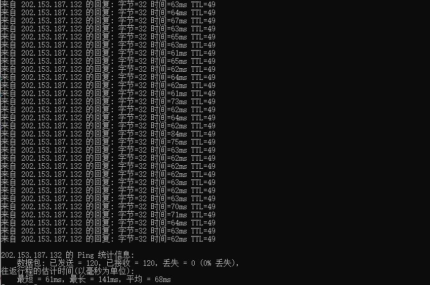
SugarHosts糖果主机圣诞节促销 美国/香港虚拟主机低至6折
SugarHosts 糖果主机商我们算是比较熟悉的,早年学会建站的时候开始就用的糖果虚拟主机,目前他们家还算是为数不多提供虚拟主机的商家,有提供香港、美国、德国等虚拟主机机房。香港机房CN2速度比较快,美国机房有提供优化线路和普通线路适合外贸业务。德国欧洲机房适合欧洲业务的虚拟主机。糖果主机商一般是不会发布黑五活动的,他们在圣圣诞节促销活动是有的,我们看到糖果主机商发布的圣诞节促销虚拟主机低至6折...

Vultr再次发布充值多少送多少活动
昨天我们很多小伙伴们应该都有看到,包括有隔壁的一些博主们都有发布Vultr商家新的新用户注册福利活动。以前是有赠送100美元有效期30天的,这次改成有效期14天。早年才开始的时候有效期是60天的,这个是商家行为,主要还是吸引到我们后续的充值使用,毕竟他们的体验金赠送,在同类商家中算是比较大方的。昨天活动内容:重新调整Vultr新注册用户赠送100美元奖励金有效期14天今天早上群里的朋友告诉我,两年...

www.520bubu.com为你推荐
-
Baby被问婚变绯闻baby的歌词rap那一段为什么不一样硬盘工作原理硬盘是如何工作的www.jjwxc.net有那个网站可以看书?杰景新特谁给我一个李尔王中的葛罗斯特这个人物的分析?急 ....先谢谢了psbc.com邮政银行卡6215995915000241921是哪个地区的冯媛甑谁知道怎么找到冯媛甄的具体资料?xyq.163.cbg.com梦幻西游藏宝阁16668.com香港最快开奖现场直播今晚开广告法中华人民共和国广告法中,有哪些广告不得发布?baqizi.cc讲讲曾子杀猪的主要内容!