STDwwwddd13com
wwwddd13com 时间:2021-04-06 阅读:()
CY2313ANZ13Output,3.
3VClockBufferCypressSemiconductorCorporation198ChampionCourtSanJose,CA95134-1709408-943-2600DocumentNumber:38-07144Rev.
*DRevisedSeptember30,201313Output,3.
3VClockBufferFeaturesOneinputto13outputbuffer/driverSupplyvoltage:3.
3VSupportsuptothreeSDRAMDIMMsSMBusserialinterfaceforoutputcontrolLowskewoutputsUpto100-MHzoperationMultipleVDDandVSSpinsfornoisereductionLowEMIoutputsPackage:28-pinsmall-outlineintegratedcircuit(SOIC)FunctionalDescriptionTheCY2313ANZisa3.
3Vclockbuffer.
WhileoriginallydesignedtodistributeclocksindesktopPCapplications-hencethesignalnames-itisageneralpurposedevicesuitabletoawidevarietyofclockbufferingapplications.
Theparthasthirteenoutputs.
InaPCapplication,twelveofwhichcanbeusedtodriveuptothreeSDRAMDIMMs,andtheremainingoutputcanbeusedforexternalfeedbacktoaPLL.
Thedeviceoperatesat3.
3Vandoutputscanrunupto100MHz.
TheCY2313ANZalsoincludesanSMBusserialinterfacewhichcanenableordisableeachoutputclock.
Onpower-up,alloutputclocksareenabled.
LogicBlockDiagramSerialInterfaceBUF_INSDATASCLOCKSDRAM0SDRAM1SDRAM2SDRAM3SDRAM4SDRAM5SDRAM6SDRAM7DecodingSDRAM8SDRAM9SDRAM10SDRAM11SDRAM12CY2313ANZDocumentNumber:38-07144Rev.
*DPage2of13ContentsPinConfiguration3PinSummary3SerialConfigurationMap4Byte0:SDRAMActive/InactiveRegister4Byte1:SDRAMActive/InactiveRegister4Byte2:SDRAMActive/InactiveRegister4MaximumRatings5OperatingConditions5ElectricalCharacteristics5SwitchingCharacteristics6SwitchingWaveforms7TestCircuit7ApplicationInformation8OrderingInformation9OrderingCodeDefinitions9PackageDiagram10Acronyms11DocumentConventions11UnitsofMeasure11DocumentHistoryPage12Sales,Solutions,andLegalInformation13WorldwideSalesandDesignSupport13Products13PSoCSolutions13CypressDeveloperCommunity13TechnicalSupport13CY2313ANZDocumentNumber:38-07144Rev.
*DPage3of13PinConfigurationFigure1.
28-pinSOICpinout(TopView)PinSummaryNamePinsDescriptionVDD1,5,20,24,283.
3VdigitalvoltagesupplyVSS4,8,17,21,25GroundVDDIIC13SerialinterfacevoltagesupplyVSSIIC16GroundforserialinterfaceBUF_IN9InputclockSDATA14SMBusdatainput/output,internalpull-uptoVDDSCLK15SMBusclockinput,internalpull-uptoVDDSDRAM[0-12]2,3,6,7,10,11,12,18,19,22,23,26,27Clockoutputs1234VDDSDRAM11SDRAM10VSSVDDSDRAM98567129101113142827262521242322172019181615SDRAM8VSSVDDSDRAM7SDRAM6VSSVSSIICSCLKVDDSDRAM0SDRAM1VSSVDDSDRAM2VSSBUF_INSDRAM4SDRAM5SDRAM12VDDIICSDATASDRAM3CY2313ANZDocumentNumber:38-07144Rev.
*DPage4of13SerialConfigurationMapTheSerialbitswillbereadbytheclockdriverinthefollowingorder:Byte0-Bits7,6,5,4,3,2,1,0Byte1-Bits7,6,5,4,3,2,1,0.
.
.
ByteN-Bits7,6,5,4,3,2,1,0Reservedandunusedbitsshouldbeprogrammedto"0"SerialinterfaceaddressfortheCY2313ANZis:A6A5A4A3A2A1A0R/W1101001–Byte0:SDRAMActive/InactiveRegister(1=Enable,0=Disable),Default=EnabledBitPin#DescriptionBit711SDRAM5(active/inactive)Bit610SDRAM4(active/inactive)Bit5–Reserved,driveto0Bit4–Reserved,driveto0Bit37SDRAM3(active/inactive)Bit26SDRAM2(active/inactive)Bit13SDRAM1(active/inactive)Bit02SDRAM0(active/inactive)Byte1:SDRAMActive/InactiveRegister(1=Active,0=Inactive),Default=ActiveBitPin#DescriptionBit727SDRAM11(active/inactive)Bit626SDRAM10(active/inactive)Bit523SDRAM9(active/inactive)Bit422SDRAM8(active/inactive)Bit3–Reserved,driveto0Bit2–Reserved,driveto0Bit119SDRAM7(active/inactive)Bit018SDRAM6(active/inactive)Byte2:SDRAMActive/InactiveRegister(1=Active,0=Inactive),Default=ActiveBitPin#DescriptionBit7–Reserved,driveto0Bit612SDRAM12(active/inactive)Bit5–Reserved,driveto0Bit4–Reserved,driveto0Bit3–Reserved,driveto0Bit2–Reserved,driveto0Bit1–Reserved,driveto0Bit0–Reserved,driveto0CY2313ANZDocumentNumber:38-07144Rev.
*DPage5of13MaximumRatingsExceedingmaximumratingsmayshortentheusefullifeofthedevice.
Userguidelinesarenottested.
Supplyvoltagetogroundpotential0.
5Vto+7.
0VDCinputvoltage(ExceptBUF_IN).
.
.
.
.
–0.
5VtoVDD+0.
5VDCinputvoltage(BUF_IN)0.
5Vto+7.
0VStoragetemperature65°Cto+150°CJunctiontemperature150°CStaticdischargevoltage(perMIL-STD-883,method3015)2000VOperatingConditionsParameter[1]DescriptionMinMaxUnitVDDSupplyvoltage3.
1353.
465VTAOperatingtemperature(ambienttemperature)070°CCLLoadcapacitance–30pFCINInputcapacitance–7pFtPUPower-uptimeforallVDD'storeachminimumspecifiedvoltage(powerrampsmustbemonotonic)0.
0550msElectricalCharacteristicsOvertheOperatingRangeParameterDescriptionTestConditionsMinMaxUnitVILInputLOWvoltage[2]Exceptserialinterfacepins–0.
8VVILiicInputLOWvoltageForserialinterfacepinsonly–0.
7VVIHInputHIGHvoltage[2]2.
0–VIILInputLOWcurrent(BUF_INinput)VIN=0V–1010AIILInputLOWcurrent(ExceptBUF_INpin)VIN=0V–100AIIHInputHIGHcurrentVIN=VDD–1010AVOLOutputLOWvoltage[3]IOL=25mA–0.
4VVOHOutputHIGHvoltage[3]IOH=–36mA2.
4–VIDDSupplycurrent[3]Unloadedoutputs,100MHz–200mAIDDSupplycurrent[3]Loadedoutputs,100MHz–290mAIDDSupplycurrent[3]Unloadedoutputs,66.
67MHz–150mAIDDSupplycurrent[3]Loadedoutputs,66.
67MHz–185mAIDDSSupplycurrentBUF_IN=VDDorVSSAllotherinputsatVDD–500ANotes1.
Electricalparametersareguaranteedundertheoperatingconditionsspecified.
2.
BUF_INinputhasathresholdvoltageofVDD/2.
3.
Parameterisguaranteedbydesignandcharacterization.
Not100%testedinproduction.
CY2313ANZDocumentNumber:38-07144Rev.
*DPage6of13SwitchingCharacteristicsOvertheOperatingRangeParameter[4]DescriptionTestConditionsMinTypMaxUnitMaximumoperatingfrequency––100MHzDutycycle[5,6]=t2t1Measuredat1.
5V455055%t3Risingedgerate[5]Measuredbetween0.
4Vand2.
4V0.
91.
54.
0V/nst4Fallingedgerate[5]Measuredbetween2.
4Vand0.
4V0.
91.
54.
0V/nst5Outputtooutputskew[5]Alloutputsequallyloaded–250–250pst6SDRAMbufferLHpropagationdelay[5]Inputedgegreaterthan1V/ns1.
03.
55.
0nst7SDRAMbufferHLpropagationdelay[5]Inputedgegreaterthan1V/ns1.
03.
55.
0nsNotes4.
Allparametersspecifiedwithloadedoutputs.
5.
Parameterisguaranteedbydesignandcharacterization.
Not100percenttestedinproduction.
6.
Dutycycleofinputclockis50percent.
Risingandfallingedgerateoftheinputclockisgreaterthan1V/ns.
CY2313ANZDocumentNumber:38-07144Rev.
*DPage7of13SwitchingWaveformsFigure2.
DutyCycleTimingFigure3.
AllOutputsRise/FallTimeFigure4.
Output-OutputSkewFigure5.
SDRAMBufferLHandHLPropagationDelayt1t21.
5V1.
5V1.
5VOUTPUT3.
3Vt30V0.
4V2.
4V2.
4V0.
4Vt41.
5Vt5OUTPUTOUTPUT1.
5Vt6INPUTOUTPUTt7TestCircuit0.
1FVDDCLKoutCLOADOUTPUTSGNDCY2313ANZDocumentNumber:38-07144Rev.
*DPage8of13ApplicationInformationClocktracesmayrequireeitherseriesorparalleltermination.
AnIBISmodelisavailableforsimulation.
Surfacemount,low-ESR,ceramiccapacitorsshouldbeusedforfiltering.
Typically,thesecapacitorshaveavalueof0.
1F.
Insomecases,smallervaluecapacitorsmayberequired.
Thevalueoftheseriesterminatingresistorsatisfiesthefollowingequation,whereRtraceistheloadedcharacteristicimpedanceofthetrace,Routistheoutputimpedanceofthebuffer(typically25),andRseriesistheseriesterminatingresistor.
Rseries>Rtrace–RoutFootprintsmustbelaidoutforoptionalEMI-reducingcapacitors,whichshouldbeplacedasclosetotheterminatingresistorasisphysicallypossible.
Typicalvaluesofthesecapacitorsrangefrom4.
7pFto22pF.
AferritebeadmaybeusedtoisolatetheboardVDDfromtheclockgeneratorVDDisland.
EnsurethattheFerriteBeadoffersgreaterthan50impedanceattheclockfrequency,underloadedDCconditions.
RefertotheapplicationnoteLayoutandTerminationTechniquesforCypressClockGeneratorsformoredetails.
IfaFerriteBeadisused,a10Fto22FtantalumbypasscapacitorshouldbeplacedclosetotheFerriteBead.
Thiscapacitorpreventspowersupplydroopduringcurrentsurges.
CY2313ANZDocumentNumber:38-07144Rev.
*DPage9of13OrderingCodeDefinitionsOrderingInformationOrderingCodePackageTypeOperatingRangeCY2313ANZSC–128-pinSOICCommercial,0°Cto70°CPb-freeCY2313ANZSXC–128-pinSOICCommercial,0°Cto70°CCY2313ANZSXC–1T28-pinSOIC–TapeandReelCommercial,0°Cto70°CT=tapeandreel,blank=tubeFixedvalueTemperatureRange:C=CommercialPackage:xx=SXorSSX=SOIC,Pb-freeS=SOIC,nonPb-freePartIdentifierCompanyCode:CY=CypressSemiconductor2313ANZCYxxC–1(T)CY2313ANZDocumentNumber:38-07144Rev.
*DPage10of13PackageDiagramFigure6.
28-pinSOIC(0.
713*0.
300*0.
0932Inches)PackageOutline,51-8502651-85026*GCY2313ANZDocumentNumber:38-07144Rev.
*DPage11of13AcronymsDocumentConventionsUnitsofMeasureAcronymDescriptionDIMMDualIn-lineMemoryModulePCPersonalComputerPLLPhase-LockedLoopSDRAMSynchronousDynamicRandomAccessMemorySOICSmall-OutlineIntegratedCircuitSymbolUnitofMeasure°CdegreeCelsiusMHzmegahertzAmicroamperemAmilliamperemsmillisecondnsnanosecondohmpFpicofaradVvoltCY2313ANZDocumentNumber:38-07144Rev.
*DPage12of13DocumentHistoryPageDocumentTitle:CY2313ANZ,13Output,3.
3VClockBufferDocumentNumber:38-07144Rev.
ECNNo.
IssueDateOrig.
ofChangeDescriptionofChange**11025311/18/01DSGChangefromSpecnumber:38-00692to38-07144*A12183112/14/02RBIPoweruprequirementsaddedtoOperatingConditionsInformation*B1244583SeeECNDPFAddedPb-freepartnumbersintheOrderingInformation*C302235509/14/2010KVMChangedtitlefrom"13Output,3.
3VSDRAMBufferforDesktopPCswithThreeDIMMs"to"13Output,3.
3VClockBuffer"ClarifiedthattheserialinterfaceisSMBusRemovedtimingparametersandwaveformsthatwerenotapplicableAddedOrderingCodeDefinitions.
UpdatedPackageDiagram.
AddedAcronymsandUnitsofMeasure.
Minoreditsandupdatedinnewtemplate*D414181009/30/2013CINMUpdatedPackageDiagram:spec51-85026–Changedrevisionfrom*Eto*G.
Updatedinnewtemplate.
CompletingSunsetReview.
DocumentNumber:38-07144Rev.
*DRevisedSeptember30,2013Page13of13PentiumisaregisteredtrademarkofIntelCorporation.
Allproductsandcompanynamesmentionedinthisdocumentmaybethetrademarksoftheirrespectiveholders.
CY2313ANZCypressSemiconductorCorporation,2001-2013.
Theinformationcontainedhereinissubjecttochangewithoutnotice.
CypressSemiconductorCorporationassumesnoresponsibilityfortheuseofanycircuitryotherthancircuitryembodiedinaCypressproduct.
Nordoesitconveyorimplyanylicenseunderpatentorotherrights.
Cypressproductsarenotwarrantednorintendedtobeusedformedical,lifesupport,lifesaving,criticalcontrolorsafetyapplications,unlesspursuanttoanexpresswrittenagreementwithCypress.
Furthermore,Cypressdoesnotauthorizeitsproductsforuseascriticalcomponentsinlife-supportsystemswhereamalfunctionorfailuremayreasonablybeexpectedtoresultinsignificantinjurytotheuser.
TheinclusionofCypressproductsinlife-supportsystemsapplicationimpliesthatthemanufacturerassumesallriskofsuchuseandindoingsoindemnifiesCypressagainstallcharges.
AnySourceCode(softwareand/orfirmware)isownedbyCypressSemiconductorCorporation(Cypress)andisprotectedbyandsubjecttoworldwidepatentprotection(UnitedStatesandforeign),UnitedStatescopyrightlawsandinternationaltreatyprovisions.
Cypressherebygrantstolicenseeapersonal,non-exclusive,non-transferablelicensetocopy,use,modify,createderivativeworksof,andcompiletheCypressSourceCodeandderivativeworksforthesolepurposeofcreatingcustomsoftwareandorfirmwareinsupportoflicenseeproducttobeusedonlyinconjunctionwithaCypressintegratedcircuitasspecifiedintheapplicableagreement.
Anyreproduction,modification,translation,compilation,orrepresentationofthisSourceCodeexceptasspecifiedaboveisprohibitedwithouttheexpresswrittenpermissionofCypress.
Disclaimer:CYPRESSMAKESNOWARRANTYOFANYKIND,EXPRESSORIMPLIED,WITHREGARDTOTHISMATERIAL,INCLUDING,BUTNOTLIMITEDTO,THEIMPLIEDWARRANTIESOFMERCHANTABILITYANDFITNESSFORAPARTICULARPURPOSE.
Cypressreservestherighttomakechangeswithoutfurthernoticetothematerialsdescribedherein.
Cypressdoesnotassumeanyliabilityarisingoutoftheapplicationoruseofanyproductorcircuitdescribedherein.
Cypressdoesnotauthorizeitsproductsforuseascriticalcomponentsinlife-supportsystemswhereamalfunctionorfailuremayreasonablybeexpectedtoresultinsignificantinjurytotheuser.
TheinclusionofCypress'productinalife-supportsystemsapplicationimpliesthatthemanufacturerassumesallriskofsuchuseandindoingsoindemnifiesCypressagainstallcharges.
UsemaybelimitedbyandsubjecttotheapplicableCypresssoftwarelicenseagreement.
Sales,Solutions,andLegalInformationWorldwideSalesandDesignSupportCypressmaintainsaworldwidenetworkofoffices,solutioncenters,manufacturer'srepresentatives,anddistributors.
Tofindtheofficeclosesttoyou,visitusatCypressLocations.
ProductsAutomotivecypress.
com/go/automotiveClocks&Bufferscypress.
com/go/clocksInterfacecypress.
com/go/interfaceLighting&PowerControlcypress.
com/go/powerpsoccypress.
com/go/plcMemorycypress.
com/go/memoryPSoCcypress.
com/go/psocTouchSensingcypress.
com/go/touchUSBControllerscypress.
com/go/USBWireless/RFcypress.
com/go/wirelessPSoCSolutionspsoc.
cypress.
com/solutionsPSoC1|PSoC3|PSoC4|PSoC5LPCypressDeveloperCommunityCommunity|Forums|Blogs|Video|TrainingTechnicalSupportcypress.
com/go/support
- STDwwwddd13com相关文档
- 公告wwwddd13com
- 南阳检察机关践行党的群众路线系列报道之四十一
- externalwwwddd13com
- 活动wwwddd13com
- 产品wwwddd13com
- 公告wwwddd13com
Linode十八周年及未来展望
这两天Linode发布了十八周年的博文和邮件,回顾了过去取得的成绩和对未来的展望。作为一家运营18年的VPS主机商,Linode无疑是有一些可取之处的,商家提供基于KVM架构的VPS主机,支持随时删除(按小时计费),可选包括美国、英国、新加坡、日本、印度、加拿大、德国等全球十多个数据中心,所有机器提供高出入网带宽,最低仅$5/月($0.0075/小时)。This month marks Linod...

无法忍受旧版不兼容PHP7+主题 更换新主题
今天父亲节我们有没有陪伴家人一起吃个饭,还是打个电话问候一下。前一段时间同学将网站账户给我说可以有空更新点信息确保他在没有时间的时候还能保持网站有一定的更新内容。不过,他这个网站之前采用的主题也不知道来源哪里,总之各种不合适,文件中很多都是他多年来手工修改的主题拼接的,并非完全适应WordPress已有的函数,有些函数还不兼容最新的PHP版本,于是每次出现问题都要去排查。于是和他商量后,就抽时间把...

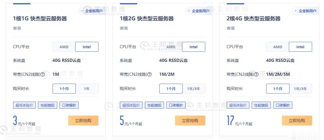
UCloud优刻得,新增1核1G内存AMD快杰云机型,服务器2元/首月,47元/年
UCloud优刻得近日针对全球大促活动进行了一次改版,这次改版更加优惠了,要比之前的优惠价格还要低一些,并且新增了1核心1G内存的快杰云服务器,2元/首年,47元/年,这个价格应该是目前市面上最低最便宜的云服务器产品了,有需要国内外便宜VPS云服务器的朋友可以关注一下。UCloud好不好,UCloud服务器怎么样?UCloud服务器值不值得购买UCloud是优刻得科技股份有限公司旗下拥有的云计算服...
wwwddd13com为你推荐
-
lunwenjiancepaperrater论文检测准确吗www.qq530.com谁能给我一个听歌的网站?www.haole012.com012.qq.com是真的吗抓站工具大家在家用什么工具练站?怎么固定?面壁思过?在医院是站站立架yinrentangweichentang产品功效好不好?33tutu.com33gan.com改成什么了bk乐乐BK乐乐和沈珂什么关系?xyq.cbg.163.com梦幻西游藏宝阁怎么开通怎么用莱姿蔓不蔓不枝的蔓是什么意思雀嘴鳝请介绍下鳄雀鳝这种鱼?