Reversewww
www.xiaomi.com 时间:2021-03-01 阅读:()
J111/J112/J113/MMBFJ111/MMBFJ112/MMBFJ113—N-ChannelSwitchPublicationOrderNumber:MMBFJ113/D1997SemiconductorComponentsIndustries,LLC.
October-2017,Rev.
2J111/J112/J113/MMBFJ111/MMBFJ112/MMBFJ113N-ChannelSwitchFeaturesThisdeviceisdesignedforlowlevelanalogswitching,sampleandholdcircuitsandchopperstabilizedamplifiers.
Sourcedfromprocess51Source&Drainareinterchangeable.
OrderingInformationFigure1.
J111/J112/J113DevicePackageFigure2.
MMBFJ111/MMBFJ112/MMBFJ113DevicePackagePartNumberTopMarkPackagePackingMethodJ111J111TO-923LBulkJ111-D26ZJ111TO-923LTapeandReelJ111-D74ZJ111TO-923LAmmoJ112J112TO-923LBulkJ112-D26ZJ112TO-923LTapeandReelJ112-D27ZJ112TO-923LTapeandReelJ112-D74ZJ112TO-923LAmmoJ113J113TO-923LBulkJ113-D74ZJ113TO-923LAmmoJ113-D75ZJ113TO-923LAmmoMMBFJ1116PSOT-233LTapeandReelMMBFJ1126RSOT-233LTapeandReelMMBFJ1136SSOT-233LTapeandReelGSDTO-92SOT-23GDSNote:Source&DrainareinterchangeableJ111/J112/J113/MMBFJ111/MMBFJ112/MMBFJ113—N-ChannelSwitchwww.
onsemi.
com2AbsoluteMaximumRatings(1),(2)Stressesexceedingtheabsolutemaximumratingsmaydamagethedevice.
Thedevicemaynotfunctionorbeopera-bleabovetherecommendedoperatingconditionsandstressingthepartstotheselevelsisnotrecommended.
Inaddi-tion,extendedexposuretostressesabovetherecommendedoperatingconditionsmayaffectdevicereliability.
Theabsolutemaximumratingsarestressratingsonly.
ValuesareatTA=25°Cunlessotherwisenoted.
Notes:1.
Theseratingsarebasedonamaximumjunctiontemperatureof150°C.
2.
Thesearesteady-statelimits.
ONSemiconductorshouldbeconsultedonapplicationsinvolvingpulsedorlow-duty-cycleoperations.
ThermalCharacteristicsValuesareatTA=25°Cunlessotherwisenoted.
Notes:3.
PCBsize:FR-4,76mmx114mmx1.
57mm(3.
0inchx4.
5inchx0.
062inch)withminimumlandpatternsize.
4.
DevicemountedonFR-4PCB36mm*18mm*1.
5mm;mountingpadforthecollectorleadminimum6cm2.
SymbolParameterValueUnitVDGDrain-GateVoltage35VVGSGate-SourceVoltage-35VIGFForwardGateCurrent50mATJ,TSTGOperatingandStorageJunctionTemperatureRange-55to150°CSymbolParameterMax.
UnitJ111/J112/J113(3)MMBFJ111/MMBFJ112/MMBFJ113(4)PDTotalDeviceDissipation625350mWDerateAbove25°C5.
02.
8mW/°CRθJCThermalResistance,Junction-to-Case125°C/WRθJAThermalResistance,Junction-to-Ambient200357°C/WJ111/J112/J113/MMBFJ111/MMBFJ112/MMBFJ113—N-ChannelSwitchElectricalCharacteristicsValuesareatTA=25°Cunlessotherwisenoted.
Note:5.
Pulsetest:pulsewidth≤300μs,dutycycle≤2%.
SymbolParameterConditionsMin.
Max.
UnitOffCharacteristicsV(BR)GSSGate-SourceBreakdownVoltageIG=-1.
0μA,VDS=0-35VIGSSGateReverseCurrentVGS=-15V,VDS=0-1.
0nAVGS(off)Gate-SourceCut-OffVoltageVDS=15V,ID=1.
0μA111-3.
0-10.
0V112-1.
0-5.
0113-0.
5-3.
0ID(off)DrainCutoffLeakageCurrentVDS=5.
0V,VGS=-10V1.
0nAOnCharacteristicsIDSSZero-GateVoltageDrainCurrent(5)VDS=15V,VGS=011120mA1125.
01132.
0rDS(on)Drain-SourceOnResistanceVDS≤0.
1V,VGS=011130Ω11250113100SmallSignalCharacteristicsCdg(on)Csg(on)Drain-Gate&Source-GateOnCapacitanceVDS=0,VGS=0,f=1.
0MHz28pFCdg(off)Drain-GateOffCapacitanceVDS=0,VGS=-10V,f=1.
0MHz5.
0pFCsg(off)Source-GateOffCapacitanceVDS=0,VGS=-10V,f=1.
0MHz5.
0pFwww.
onsemi.
com3J111/J112/J113/MMBFJ111/MMBFJ112/MMBFJ113—N-ChannelSwitchTypicalPerformanceCharacteristicsFigure3.
CommonDrain-SourceFigure4.
ParameterInteractionsFigure5.
TransferCharacteristicsFigure6.
TransferCharacteristicsFigure7.
TransferCharacteristicsFigure8.
TransferCharacteristics00.
40.
81.
21.
620246810V-DRAIN-SOURCEVOLTAGE(V)I-DRAINCURRENT(mA)DSD-0.
4V-1.
0V-0.
8V-0.
2V-0.
6VV=0VGST=25°CTYPV=-2.
0VGS(off)A-1.
2V-1.
4Vr-DRAIN"ON"RESISTANCE(ΩΩ)0.
51251051020501005102050100V-GATECUTOFFVOLTAGE(V)g-TRANSCONDUCTANCE(mmhos)GS(OFF)fsI,g@V=15V,V=0PULSEDr@1.
0mA,V=0V@V=15V,I=1.
0nAGS(off)DSSrDIDSSDSDSGSDSDSGSfsDSDSgfs_____-3-2-10010203040V-GATE-SOURCEVOLTAGE(V)I-DRAINCURRENT(mA)GSDV=-3.
0VGS(off)25°CV=15VDSV=-2.
0VGS(off)125°C-55°C25°C-55°C125°C-1.
5-1-0.
500481216V-GATE-SOURCEVOLTAGE(V)I-DRAINCURRENT(mA)GSDV=-1.
6VGS(off)25°CV=15VDSV=-1.
1VGS(off)125°C-55°C25°C-55°C125°C-3-2-100102030V-GATE-SOURCEVOLTAGE(V)g-TRANSCONDUCTANCE(mmhos)GSfsV=-3.
0VGS(off)25°CV=15VDSV=-2.
0VGS(off)125°C-55°C25°C125°C-55°C-1.
5-1-0.
500102030V-GATE-SOURCEVOLTAGE(V)g-TRANSCONDUCTANCE(mmhos)GSfsV=-1.
6VGS(off)25°CV=15VDSV=-1.
1VGS(off)125°C-55°C25°C125°C-55°Cwww.
onsemi.
com4J111/J112/J113/MMBFJ111/MMBFJ112/MMBFJ113—N-ChannelSwitchTypicalPerformanceCharacteristics(Continued)Figure9.
OnResistancevs.
DrainCurrentFigure10.
NormalizedDrainResistancevs.
BiasVoltageFigure11.
Transconductancevs.
DrainCurrentFigure12.
OutputConductancevs.
DrainCurrentFigure13.
Capacitancevs.
VoltageFigure14.
NoiseVoltagevs.
Frequency125102050100102050100I-DRAINCURRENT(mA)r-DRAIN"ON"RESISTANCEDDSVTYP=-7.
0VGS(off)25°C(Ω)125°C25°C125°Cr@V=0GS-55°CDSVTYP=-2.
0VGS(off)-55°C00.
20.
40.
60.
81125102050100V/V-NORMALIZEDGATE-SOURCEVOLTAGE(V)r-NORMALIZEDRESISTANCEGSDSr=DSV@5.
0V,10μAGS(off)rDS________VGS(off)VGS1-GS(off)(Ω)Ω)Ω)Ω)Ω)0.
1110110100I-DRAINCURRENT(mA)g-TRANSCONDUCTANCE(mmhos)DfsV=-1.
4VGS(off)T=25°CV=15Vf=1.
0kHzADGV=-3.
0VGS(off)0.
010.
1100.
1110100I-DRAINCURRENT(mA)g-OUTPUTCONDUCTANCE(mhos)DosV=-5.
0VGS(off)T=25°Cf=1.
0kHzV=5.
0VDGμA10V15V20V5.
0VV=-2.
0VGS(off)V=-0.
85VGS(off)10V15V20V10V15V20V5.
0V-20-16-12-8-40110100V-GATE-SOURCEVOLTAGE(V)C(C)-CAPACITANCE(pF)rsGSisC(V=0)isDSC(V=20)isDSC(V=0)rsDSf=0.
1-1.
0MHz0.
01110100151050100f-FREQUENCY(kHz)e-NOISEVOLTAGE(nV/Hz)nV=15VBW=6.
0Hz@f=10Hz,100Hz=0.
21@f≥1.
0kHzDGI=10mADI=1.
0mAD√www.
onsemi.
com5J111/J112/J113/MMBFJ111/MMBFJ112/MMBFJ113—N-ChannelSwitchTypicalPerformanceCharacteristics(Continued)Figure15.
NoiseVoltagevs.
CurrentFigure16.
PowerDissipationvs.
AmbientTemperatureFigure17.
SwitchingTurn-OnTimevs.
Gate-SourceVoltageFigure18.
SwitchingTurn-OffTimevs.
DrainCurrent0.
010.
1110110100I-DRAINCURRENT(mA)e-NOISEVOLTAGE(nV/Hz)nV=15VDG√Df=10Hzf=100Hzf=1.
0kHzf=10kHzf=100kHz02550751001251500100200300400500600700TEMPERATURE(C)P-POWERDISSIPATION(mW)DoTO-92SOT-23-10-8-6-4-200510152025V-GATE-SOURCECUTOFFVOLTAGE(V)t,t-TURN-ONTIME(ns)r(ON)GS(off)d(ON)V=3.
0VtAPPROX.
IINDEPENDENTDDDrV=3.
0VT=25°CGS(off)AI=6.
6mAV=-12VDGStr(ON)td(ON)2.
5mA-6.
0V0246810020406080100I-DRAINCURRENT(mA)t,t-TURN-OFFTIME(ns)Dd(OFF)OFFT=25°CV=3.
0VV=-12VtDEVICEVINDEPENDENTGS(off)ADDGSd(off)V=-2.
2VGS(off)-4.
0V-7.
5Vtd(off)t(off)www.
onsemi.
com6J111/J112/J113/MMBFJ111/MMBFJ112/MMBFJ113—N-ChannelSwitchPhysicalDimensionsFigure19.
3-Lead,TO-92,JEDECTO-92CompliantStraightLeadConfiguration,BulkTypeDwww.
onsemi.
com7J111/J112/J113/MMBFJ111/MMBFJ112/MMBFJ113—N-ChannelSwitchPhysicalDimensions(Continued)Figure20.
3-Lead,TO-92,Molded,0.
2InLineSpacingLeadForm,Ammo,TapeandReelTypewww.
onsemi.
com8J111/J112/J113/MMBFJ111/MMBFJ112/MMBFJ113—N-ChannelSwitchPhysicalDimensions(Continued)Figure21.
3-LEAD,SOT23,JEDECTO-236,LOWPROFILELANDPATTERNRECOMMENDATIONNOTES:UNLESSOTHERWISESPECIFIEDA)REFERENCEJEDECREGISTRATIONTO-236,VARIATIONAB,ISSUEH.
B)ALLDIMENSIONSAREINMILLIMETERS.
C)DIMENSIONSAREINCLUSIVEOFBURRS,MOLDFLASHANDTIEBAREXTRUSIONS.
D)DIMENSIONINGANDTOLERANCINGPERASMEY14.
5M-1994.
E)DRAWINGFILENAME:MA03DREV10312SEEDETAILASEATINGPLANESCALE:2XGAGEPLANE(0.
55)(0.
93)1.
20MAXC0.
100.
000.
10C2.
40±0.
302.
92±0.
201.
30+0.
20-0.
150.
600.
370.
20AB1.
900.
95(0.
29)0.
951.
402.
201.
001.
900.
250.
230.
080.
20MINwww.
onsemi.
com9ONSemiconductorandaretrademarksofSemiconductorComponentsIndustries,LLCdbaONSemiconductororitssubsidiariesintheUnitedStatesand/orothercountries.
ONSemiconductorownstherightstoanumberofpatents,trademarks,copyrights,tradesecrets,andotherintellectualproperty.
AlistingofONSemiconductor'sproduct/patentcoveragemaybeaccessedatwww.
onsemi.
com/site/pdf/PatentMarking.
pdf.
ONSemiconductorreservestherighttomakechangeswithoutfurthernoticetoanyproductsherein.
ONSemiconductormakesnowarranty,representationorguaranteeregardingthesuitabilityofitsproductsforanyparticularpurpose,nordoesONSemiconductorassumeanyliabilityarisingoutoftheapplicationoruseofanyproductorcircuit,andspecificallydisclaimsanyandallliability,includingwithoutlimitationspecial,consequentialorincidentaldamages.
BuyerisresponsibleforitsproductsandapplicationsusingONSemiconductorproducts,includingcompliancewithalllaws,regulationsandsafetyrequirementsorstandards,regardlessofanysupportorapplicationsinformationprovidedbyONSemiconductor.
"Typical"parameterswhichmaybeprovidedinONSemiconductordatasheetsand/orspecificationscananddovaryindifferentapplicationsandactualperformancemayvaryovertime.
Alloperatingparameters,including"Typicals"mustbevalidatedforeachcustomerapplicationbycustomer'stechnicalexperts.
ONSemiconductordoesnotconveyanylicenseunderitspatentrightsnortherightsofothers.
ONSemiconductorproductsarenotdesigned,intended,orauthorizedforuseasacriticalcomponentinlifesupportsystemsoranyFDAClass3medicaldevicesormedicaldeviceswithasameorsimilarclassificationinaforeignjurisdictionoranydevicesintendedforimplantationinthehumanbody.
ShouldBuyerpurchaseoruseONSemiconductorproductsforanysuchunintendedorunauthorizedapplication,BuyershallindemnifyandholdONSemiconductoranditsofficers,employees,subsidiaries,affiliates,anddistributorsharmlessagainstallclaims,costs,damages,andexpenses,andreasonableattorneyfeesarisingoutof,directlyorindirectly,anyclaimofpersonalinjuryordeathassociatedwithsuchunintendedorunauthorizeduse,evenifsuchclaimallegesthatONSemiconductorwasnegligentregardingthedesignormanufactureofthepart.
ONSemiconductorisanEqualOpportunity/AffirmativeActionEmployer.
Thisliteratureissubjecttoallapplicablecopyrightlawsandisnotforresaleinanymanner.
PUBLICATIONORDERINGINFORMATIONN.
AmericanTechnicalSupport:8002829855TollFreeUSA/CanadaEurope,MiddleEastandAfricaTechnicalSupport:Phone:421337902910JapanCustomerFocusCenterPhone:81358171050www.
onsemi.
comLITERATUREFULFILLMENT:LiteratureDistributionCenterforONSemiconductor19521E.
32ndPkwy,Aurora,Colorado80011USAPhone:3036752175or8003443860TollFreeUSA/CanadaFax:3036752176or8003443867TollFreeUSA/CanadaEmail:orderlit@onsemi.
comONSemiconductorWebsite:www.
onsemi.
comOrderLiterature:http://www.
onsemi.
com/orderlitForadditionalinformation,pleasecontactyourlocalSalesRepresentativeSemiconductorComponentsIndustries,LLC
- Reversewww相关文档
- 当事人www.xiaomi.com
- www.xiaomi.comi.xiaomi.com为什么进入了打不开什么也看不到
- www.xiaomi.com小米官网网址是?
- www.xiaomi.com小米序列号查询
- www.xiaomi.com为什么打开不了小米官网呢!!出现错误404
湖北50G防御物理服务器( 199元/月 ),国内便宜的高防服务器
4324云是成立于2012年的老牌商家,主要经营国内服务器资源,是目前国内实力很强的商家,从价格上就可以看出来商家实力,这次商家给大家带来了全网最便宜的物理服务器。只能说用叹为观止形容。官网地址 点击进入由于是活动套餐 本款产品需要联系QQ客服 购买 QQ 800083597 QQ 2772347271CPU内存硬盘带宽IP防御价格e5 2630 12核16GBSSD 500GB30M1个IP...

.asia域名是否适合做个人网站及.asia域名注册和续费成本
今天看到群里的老秦同学在布局自己的网站项目,这个同学还是比较奇怪的,他就喜欢用这些奇怪的域名。比如前几天看到有用.in域名,个人网站他用的.me域名不奇怪,这个还是常见的。今天看到他在做的一个范文网站的域名,居然用的是 .asia 后缀。问到其理由,是有不错好记的前缀。这里简单的搜索到.ASIA域名的新注册价格是有促销的,大约35元首年左右,续费大约是80元左右,这个成本算的话,比COM域名还贵。...

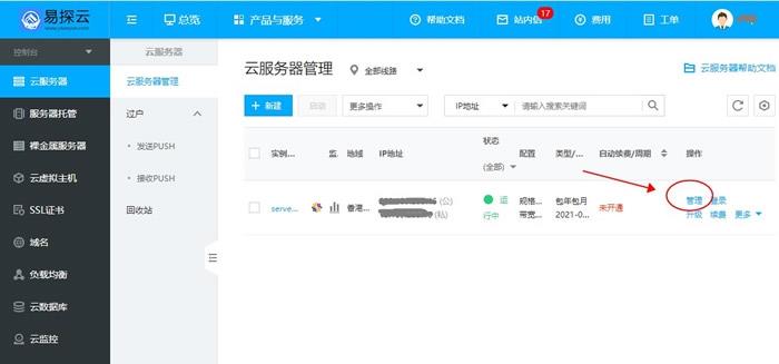
易探云服务器怎么过户/转让?云服务器PUSH实操步骤
易探云服务器怎么过户/转让?易探云支持云服务器PUSH功能,该功能可将云服务器过户给指定用户。可带价PUSH,收到PUSH请求的用户在接收云服务器的同时,系统会扣除接收方的款项,同时扣除相关手续费,然后将款项打到发送方的账户下。易探云“PUSH服务器”的这一功能,可以让用户将闲置云服务器转让给更多需要购买的用户!易探云服务器怎么过户/PUSH?1.PUSH双方必须为认证用户:2.买家未接收前,卖家...
www.xiaomi.com为你推荐
-
今日油条油条是怎样由来同ip站点查询如何查看几个站是不是同IP777k7.comwww.777tk.com.怎么打不 开郭泊雄郭佰雄最后一次出现是什么时候?www.765.com下载小说地址www.baitu.com谁有免费的动漫网站?百度指数词百度指数我创建的新词lcoc.top日本Ni-TOP是什么意思?bbs2.99nets.com西安论坛、西安茶馆网、西安社区、西安bbs 的网址是多少?kb123.netwww.zhmmjyw.net百度收录慢?