capacitorncp
ncp 时间:2021-01-11 阅读:()
SemiconductorComponentsIndustries,LLC,2014December,2014Rev.
11PublicationOrderNumber:NCP456/DNCP456R,NCP4572ASingleLoadSwitchforLowVoltageRailTheNCP456RandNCP457arepowerloadswitchwithverylowRonNMOSFETcontrolledbyexternallogicpin,allowingoptimizationofbatterylife,andportabledeviceautonomy.
Indeed,thankstoabestinclasscurrentconsumptionoptimizationwithNMOSstructure,leakagecurrentsaredrasticallydecreased.
OfferingoptimizedleakagesisolationontheICsconnectedonthebattery.
Outputdischargepathisproposed,intheNCP457version,toeliminateresidualvoltagesontheexternalcomponentsconnectedonoutputpin.
Reversevoltageprotection,fromOUTtoINisofferedintheNCP456Rversion.
Proposedinwideinputvoltagerangefrom0.
75Vto5.
5V,andaverysmallCSP60.
85x1.
25mm2.
Features0.
75V5.
5VOperatingRange24mWNMOSFETVbiasRailInputDCCurrentupto2AOutputAutodischargeOptionReverseBlockingOptionActiveHighENPinCSP6,0.
85x1.
25mm2,Pitch0.
4mmTheseDevicesarePbFreeandareRoHSCompliantTypicalApplicationsNotebooksTabletsWirelessMobilePhonesDigitalCamerasENxEN0DCDCConverterV+PlatformIC'nLDOLSorSMPSVccNCP456xNCP457INB1GateA2VbiasC1GNDC2ENA1OUTB2Figure1.
TypicalApplicationSchematichttp://onsemi.
comMARKINGDIAGRAMWLCSP6,1.
25x0.
85CASE567GZSeedetailedordering,markingandshippinginformationonpage12ofthisdatasheet.
ORDERINGINFORMATIONPINCONNECTIONSA=AssemblyLocationY=YearW=WorkWeekXXAYW12ABCENGateINVIBASOUTGNDTopViewNCP456R,NCP457http://onsemi.
com2ENxEN0DCDCConverterPlatformIC'nLDOLSorNCP456xNCP457INB1GateA2VbiasC1GNDC2ENA1OUTB2Figure2.
ApplicationSchematicwithVbiasConnectedtoINandNoGateDelayPINFUNCTIONDESCRIPTIONPinNamePinNumberTypeDescriptionENA1INPUTEnableinput,logichighturnsonpowerswitch.
INB1POWERLoadswitchinputpin.
VBIASC1POWERExternalsupplyvoltageinput.
GATEA2INPUTOUTpinslewratecontrol(trise).
OUTB2POWERLoadswitchoutputpin.
GNDC2POWERGroundconnection.
NCP456R,NCP457http://onsemi.
com3BLOCKDIAGRAMSControllogic&ChargePumpGatedriverIN:B1EN:A1OUT:B2GND:C2VBIAS:C1GATE:A2Figure3.
NCP456RBlockDiagramNCP456RVersionControllogic&ChargePumpGatedriverIN:B1EN:A1OUT:B2GND:C2VBIAS:C1GATE:A2Figure4.
NCP457BlockDiagramNCP457VersionNCP456R,NCP457http://onsemi.
com4MAXIMUMRATINGSRatingSymbolValueUnitIN,OUT,EN,VBIAS,GATEPins:(Note1)VEN,VIN,VOUT,VBIAS,VGATE0.
3to+6.
5VFromINtoOUTPins:Input/Output(Note1)NCP457VIN,VOUT0to+6.
5VFromINtoOUTPins:Input/Output(Note1)NCP456RVIN,VOUT±6.
5VHumanBodyModel(HBM)ESDRatingare(Note2)ESDHBM2000VMachineModel(MM)ESDRatingare(Note2)ESDMM200VLatchupProtection(Note3)PinsIN,OUT,EN,VBIASandGATELU100mAMaximumJunctionTemperatureTJ40to+125°CStorageTemperatureRangeTSTG40to+150°CMoistureSensitivity(Note4)MSLLevel1StressesexceedingthoselistedintheMaximumRatingstablemaydamagethedevice.
Ifanyoftheselimitsareexceeded,devicefunctionalityshouldnotbeassumed,damagemayoccurandreliabilitymaybeaffected.
1.
AccordingtoJEDECstandardJESD22A108.
2.
ThisdeviceseriescontainsESDprotectionandpassesthefollowingtests:HumanBodyModel(HBM)±2.
0kVperJEDECstandard:JESD22A114forallpins.
MachineModel(MM)±250VperJEDECstandard:JESD22A115forallpins.
3.
LatchupCurrentMaximumRating:±100mAperJEDECstandard:JESD78classII.
4.
MoistureSensitivityLevel(MSL):1perIPC/JEDECstandard:JSTD020.
OPERATINGCONDITIONSSymbolParameterConditionsMinTypMaxUnitVINOperationalPowerSupply0.
755.
5VVENEnableVoltage05.
5VVBIASBiasvoltage(VBIAS≥bestofVIN,Vout)1.
25.
5VTAAmbientTemperatureRange4025+85°CCINDecouplinginputcapacitor100nFCOUTDecouplingoutputcapacitor100nFRqJAThermalResistanceJunctiontoAirCSP6(Note5)100°C/WIOUTMaximumDCcurrent2APDPowerDissipationRating(Note6)0.
2WFunctionaloperationabovethestresseslistedintheRecommendedOperatingRangesisnotimplied.
ExtendedexposuretostressesbeyondtheRecommendedOperatingRangeslimitsmayaffectdevicereliability.
5.
TheRqJAisdependentofthePCBheatdissipationandthermalvia.
6.
Themaximumpowerdissipation(PD)isgivenbythefollowingformula:PD+TJMAX*TARqJANCP456R,NCP457http://onsemi.
com5ELECTRICALCHARACTERISTICSMin&MaxLimitsapplyforTAbetween40°Cto+85°CforVINandVBIASbetween0.
75Vto5.
5V(Unlessotherwisenoted).
TypicalvaluesarereferencedtoTA=+25°C,VIN=3.
3VandVBIAS=5V(Unlessotherwisenoted).
SymbolParameterConditionsMinTypMaxUnitPOWERSWITCHRDS(on)StaticdrainsourceonstateresistanceforeachrailVIN=VBIAS=5.
5VTA=25°C2433mWTJ=125°C39mWVIN=VBIAS=3.
3VTA=25°C2433TJ=125°C39VIN=VBIAS=1.
8VTA=25°C2534TJ=125°C40VIN=VBIAS=1.
5VTA=25°C2635TJ=125°C41VIN=VBIAS=1.
2VTA=25°C2840TJ=125°C42VIN=1.
0V.
VBIAS=1.
2VTA=25°C3040TJ=125°C42VIN=0.
8V,VBIAS=1.
2VTA=25°C3545TJ=125°C50RDISOutputdischargepathEN=low,NCP457220WTIMINGSTROutputrisetimeVIN=5VNocaponGATEpin0.
11msGatecapacitor=1nF1.
4Gatecapacitor=10nF15.
7TFOutputfalltimeCLOAD=1mF,RLOAD=25W(Note8)50msTenEnabletimeFromENlowtohightoVout=10%offullyonNCP456R.
10nFgatecapacitor3msFromENlowtohightoVout=10%offullyonNCP456R.
1nFgatecapacitor300msFromENlowtohightoVout=10%offullyonNCP456R.
Withoutgatecapacitor51msProductparametricperformanceisindicatedintheElectricalCharacteristicsforthelistedtestconditions,unlessotherwisenoted.
ProductperformancemaynotbeindicatedbytheElectricalCharacteristicsifoperatedunderdifferentconditions.
7.
ParametersareguaranteedforCLOADandRLOADconnectedtotheOUTpinwithrespecttotheground8.
Guaranteedbydesignandcharacterization,notproductiontested.
NCP456R,NCP457http://onsemi.
com6ELECTRICALCHARACTERISTICSMin&MaxLimitsapplyforTAbetween40°Cto+85°CforVINandVBIASbetween0.
75Vto5.
5V(Unlessotherwisenoted).
TypicalvaluesarereferencedtoTA=+25°C,VIN=3.
3VandVBIAS=5V(Unlessotherwisenoted).
SymbolUnitMaxTypMinConditionsParameterTIMINGSTROutputrisetimeVIN=3.
3VNocaponGATEpin0.
10.
3msGatecapacitor=1nF1Gatecapacitor=10nF11TFOutputfalltimeCLOAD=1mF,RLOAD=25W(Note8)60120msTenEnabletimeFromENlowtohightoVout=10%offullyonNCP456R.
10nFGatecapacitor.
2.
4msFromENlowtohightoVout=10%offullyonNCP456R.
1nFGatecapacitor.
230msFromENlowtohightoVout=10%offullyonNCP456R.
Withoutgatecapacitor50120msTROutputrisetimeVIN=1.
8VNocaponGATEpin0.
06msGatecapacitor=1nF0.
6Gatecapacitor=10nF6TFOutputfalltimeCLOAD=1mF,RLOAD=25W(Note8)35msTenEnabletimeFromENlowtohightoVout=10%offullyon10nFGatecapacitor1.
8msFromENlowtohightoVout=10%offullyon1nFGatecapacitor180msFromENlowtohightoVout=10%offullyonNCP456R.
Withoutgatecapacitor42msTROutputrisetimeVIN=1VNocaponGATEpin0.
04msGatecapacitor=1nF0.
35Gatecapacitor=10nF3.
5TFOutputfalltimeCLOAD=1mF,RLOAD=25W(Note8)20msTenEnabletimeFromENlowtohightoVout=10%offullyonNCP456R.
1nFgatecapacitor140msFromENlowtohightoVout=10%offullyonNCP456R.
Withoutgatecapacitor40msLOGICVIHHighlevelinputvoltage0.
9VVILLowlevelinputvoltage0.
4VRENPulldownresistor37MWProductparametricperformanceisindicatedintheElectricalCharacteristicsforthelistedtestconditions,unlessotherwisenoted.
ProductperformancemaynotbeindicatedbytheElectricalCharacteristicsifoperatedunderdifferentconditions.
7.
ParametersareguaranteedforCLOADandRLOADconnectedtotheOUTpinwithrespecttotheground8.
Guaranteedbydesignandcharacterization,notproductiontested.
NCP456R,NCP457http://onsemi.
com7ELECTRICALCHARACTERISTICSMin&MaxLimitsapplyforTAbetween40°Cto+85°CforVINandVBIASbetween0.
75Vto5.
5V(Unlessotherwisenoted).
TypicalvaluesarereferencedtoTA=+25°C,VIN=3.
3VandVBIAS=5V(Unlessotherwisenoted).
SymbolUnitMaxTypMinConditionsParameterREVERSECURRENTBLOCKINGVrev_thrReversethresholdVoutVin32mVVrev_hystReversethresholdhysteresis50mVTrevReversecompara-torresponsetimeVoutVin>Vrev_thr2.
5msQUIESCENTCURRENTNCP456RIVBIASBiascurrentforchargepumpVBIAS=3.
3V,EN=high1.
56mAIININCurrentcon-sumptionEN=high0.
010.
3mAISTBStandbycurrentINEN=low,INstandbycurrent,VIN=3.
3V0.
010.
3mAISTDVbiasStandbycurrentVBIASVBIAS=3.
3VEN=low0.
42mAIout_leakOutputleakagecurrentINconnectedtoGND,VOUT=5V0.
010.
5mAQUIESCENTCURRENTNCP457IVBIASBiascurrentforchargepumpVBIAS=3.
3V,EN=high1.
35mAIQINCurrentcon-sumptionEN=high0.
010.
3mAISTBStandbycurrentINEN=low,INstandbycurrent,VIN=3.
3V0.
011.
6mAISTDVbiasStandbycurrentVBIASVBIAS=3.
3VEN=low0.
42mAProductparametricperformanceisindicatedintheElectricalCharacteristicsforthelistedtestconditions,unlessotherwisenoted.
ProductperformancemaynotbeindicatedbytheElectricalCharacteristicsifoperatedunderdifferentconditions.
7.
ParametersareguaranteedforCLOADandRLOADconnectedtotheOUTpinwithrespecttotheground8.
Guaranteedbydesignandcharacterization,notproductiontested.
NCP456R,NCP457http://onsemi.
com8TIMINGSTONTENTRTDISTFVoutENVinTOFFFigure5.
Enable,RiseandFallTimeNCP456R,NCP457http://onsemi.
com9TYPICALCHARACTERISTICSFigure6.
RDS(on)versusVin,RoomTemperature,Vbias5VFigure7.
RDS(on)versusVin,RoomTemperature,VbiasConnectedtoVinNCP456R,NCP457http://onsemi.
com10FUNCTIONALDESCRIPTIONOverviewTheNCP456RandNCP457arehighsideNChannelMOSFETpowerdistributionswitchdesignedtoisolateICsconnectedonthebatteryorDCDCsuppliesinordertosaveenergy.
Thepartcanbeusedwithawiderangeofsupplyfrom0.
75Vto5.
5V.
EnableinputEnablepinisanactivehigh.
ThepathisopenedwhenENpinistiedlow(disable),forcingNMOSswitchoff.
TheIN/OUTpathisactivatedwithaminimumofVBIAS≥bestofVIN,VOUT=0.
75VandENforcedtohighlevel.
AutoDischarge(OptionalNCP457)NMOSFETisplacedbetweentheoutputpinandGND,inordertodischargetheapplicationcapacitorconnectedonOUTpin.
TheautodischargeisactivatedwhenENpinissettolowlevel(disablestate).
Thedischargepath(PulldownNMOS)staysactivatedaslongasENpinissetatlowlevelandVBIAS>0.
75V.
InordertolimitthecurrentacrosstheinternaldischargeNMOSFET,thetypicalvalueissetat220W.
VBIASRailThecoreoftheICissuppliedduetoVBIASsupplyrail(common+5V,3.
3V,1.
8V,1.
2V.
.
.
etc).
Indeed,nocurrentconsumptionisusedonINpin,allowingtoimprovepowersavingoftherailthatmustbeisolatedbythepowerswitch.
IfVbiasrailisnotavailableorused,VbiaspinandVinpincanbeconnectedtogheterascloseaspossibletheDUT.
OutputRiseTimeGateControlTheNMOSiscontrolwithinternalchargepumpanddriver.
AminimumgateslewrateisinternallysettoavoidhugeinrushcurrentwhenENissetfromlowtohigh.
ThedefaultgateslewratedependsonVinlevel.
ThehigherVinlevel,thelongerrisetime.
Inaddition,anexternalcapacitorcanbeconnectedbetweenGatepinandGNDinordertoslowdownthegaterising.
Seeelectricaltableformoredetails.
CinandCoutCapacitors100nFexternalcapacitorsmustbeconnectedascloseaspossibletheDUTfornoiseimmunityandbetterstability.
Incaseofinputhotplug(inputvoltageconnectedwithfastslewratefewmsit'sstronglyrecommendedtoavoidbigcapacitorconnectedontheinput.
Thatallowstoavoidinputovervoltagetransients.
ReverseBlockingControl(OptionalNCP456R)AreverseblockingcontrolcircuitryisembeddedtoeliminateleakagesfromOUTtoINincaseofVout>Vin.
AcomparatormeasuresthedropoutvoltageontheswitchbetweenOUTandINandturnofftheNMOSifthisvoltageexceedsspecifiedreversevoltage.
ThiscomparatorisavailablewhatevertheENpinlevel.
APPLICATIONINFORMATIONPowerDissipationMaincontributorintermofjunctiontemperatureisthepowerdissipationofthepowerMOSFET.
Assumingthis,thepowerdissipationandthejunctiontemperatureinnormalmodecanbecalculatedwiththefollowingequations:PD+RDS(on)ǒIout2(eq.
1)PD=Powerdissipation(W)RDS(on)=PowerMOSFETonresistance(W)Iout=Outputcurrent(A)TJ+RDRqJA)TA(eq.
2)TJ=Junctiontemperature(°C)RqJA=Packagethermalresistance(°C/W)TA=Ambienttemperature(°C)DemoboardTheNCP456RandNCP457integratea2AratedNMOSFET,andthePCBrulesmustberespectedtoproperlyevacuatetheheatoutofthesilicon.
ThepackageisaCSPandduetothelowthermalresistanceofthesilicon,alltheballscanbeusedtoimprovedpowerdissipation.
Indeed,evenifthepowercrossestheIN/OUTpinsonly,alltheballsaroundthispowerareashouldbeconnectedtothelargerPCBarea.
InthebelowPCBexample(applicationdemonstrationboard),allthePCBareasconnectedto6ballsareenlarged.
InadditionviasareconnectedtobottomsidewithexactlysameformfactoroftheotherPCBside.
Additionalimprovementscanbedonealsobyusingmorecopperthicknessandthethinnerepoxyaspossible.
NCP456R,NCP457http://onsemi.
com11Figure8.
PCBTopViewFigure9.
PCBBottomViewJ9Bat12R3100kGND12INC11μFGND12D1DIODEZENER1D2DIODEZENER1IN_2R2100kC21μFU1NCP456xNCP457INB1GateA2VbiasC1GNDC2ENA1OUTB2C31nFOUTC41μFVBIASENOUT_2Figure10.
BoardSchematicNCP456R,NCP457http://onsemi.
com12BILLOFMATERIALQuantityReferenceschemPartdescriptionPartnumberManufacturer2IN,OUTSocket,4mm,metal,PK5B010HIRSCHMANN4IN_2,OUT_2,VBIAS,ENHEADER2002.
54mm,77313-101-06LFFC1J9(Bat)HEADER200-22.
54mm,77313-101-06LFFC3C1,C2,C41uFGRM155R70J105KA12#Murata1C31nF,NotmountedGRM188R60J102ME47#Murata1D1,D2TVSESD9xONsemiconductor2GND2,GNDGNDJUMPERD3082F05Harvin2R2,R3Resistor100k0603MC0.
06306031%100KMULTICOMP1U1LoadswitchNCP456-457ONsemiconductorORDERINGINFORMATIONDeviceOptionsMarkingPackageShippingNCP456RFCCT2GReverseVoltageProtection56dYWWLCSP1.
25x0.
85mm(PbFree)3000Tape/ReelNCP457FCT2GDischargePath57dYWWLCSP1.
25x0.
85mm(PbFree)3000Tape/ReelForinformationontapeandreelspecifications,includingpartorientationandtapesizes,pleaserefertoourTapeandReelPackagingSpecificationsBrochure,BRD8011/D.
NCP456R,NCP457http://onsemi.
com13PACKAGEDIMENSIONSWLCSP6,1.
25x0.
85CASE567GZISSUEBSEATINGPLANE0.
25CNOTES:1.
DIMENSIONINGANDTOLERANCINGPERASMEY14.
5M,1994.
2.
CONTROLLINGDIMENSION:MILLIMETERS.
3.
COPLANARITYAPPLIESTOTHESPHERICALCROWNSOFTHESOLDERBALLS.
2XDIMAMINMAXMILLIMETERSA1D1.
25BSCEb0.
240.
29e0.
40BSC0.
62DEABPINA1REFERENCEeA0.
05BC0.
03C0.
05C6Xb120.
10CA1A2C0.
170.
230.
85BSC0.
256XDIMENSIONS:MILLIMETERS*ForadditionalinformationonourPbFreestrategyandsolderingdetails,pleasedownloadtheONSemiconductorSolderingandMountingTechniquesReferenceManual,SOLDERRM/D.
SOLDERINGFOOTPRINT*0.
400.
25C2XTOPVIEWSIDEVIEWBOTTOMVIEWNOTE3A20.
36REFRECOMMENDEDA1PACKAGEOUTLINEABCPITCH0.
40PITCHAee/2ONSemiconductorandareregisteredtrademarksofSemiconductorComponentsIndustries,LLC(SCILLC).
SCILLCownstherightstoanumberofpatents,trademarks,copyrights,tradesecrets,andotherintellectualproperty.
AlistingofSCILLC'sproduct/patentcoveragemaybeaccessedatwww.
onsemi.
com/site/pdf/PatentMarking.
pdf.
SCILLCreservestherighttomakechangeswithoutfurthernoticetoanyproductsherein.
SCILLCmakesnowarranty,representationorguaranteeregardingthesuitabilityofitsproductsforanyparticularpurpose,nordoesSCILLCassumeanyliabilityarisingoutoftheapplicationoruseofanyproductorcircuit,andspecificallydisclaimsanyandallliability,includingwithoutlimitationspecial,consequentialorincidentaldamages.
"Typical"parameterswhichmaybeprovidedinSCILLCdatasheetsand/orspecificationscananddovaryindifferentapplicationsandactualperformancemayvaryovertime.
Alloperatingparameters,including"Typicals"mustbevalidatedforeachcustomerapplicationbycustomer'stechnicalexperts.
SCILLCdoesnotconveyanylicenseunderitspatentrightsnortherightsofothers.
SCILLCproductsarenotdesigned,intended,orauthorizedforuseascomponentsinsystemsintendedforsurgicalimplantintothebody,orotherapplicationsintendedtosupportorsustainlife,orforanyotherapplicationinwhichthefailureoftheSCILLCproductcouldcreateasituationwherepersonalinjuryordeathmayoccur.
ShouldBuyerpurchaseoruseSCILLCproductsforanysuchunintendedorunauthorizedapplication,BuyershallindemnifyandholdSCILLCanditsofficers,employees,subsidiaries,affiliates,anddistributorsharmlessagainstallclaims,costs,damages,andexpenses,andreasonableattorneyfeesarisingoutof,directlyorindirectly,anyclaimofpersonalinjuryordeathassociatedwithsuchunintendedorunauthorizeduse,evenifsuchclaimallegesthatSCILLCwasnegligentregardingthedesignormanufactureofthepart.
SCILLCisanEqualOpportunity/AffirmativeActionEmployer.
Thisliteratureissubjecttoallapplicablecopyrightlawsandisnotforresaleinanymanner.
PUBLICATIONORDERINGINFORMATIONN.
AmericanTechnicalSupport:8002829855TollFreeUSA/CanadaEurope,MiddleEastandAfricaTechnicalSupport:Phone:421337902910JapanCustomerFocusCenterPhone:81358171050NCP456/DLITERATUREFULFILLMENT:LiteratureDistributionCenterforONSemiconductorP.
O.
Box5163,Denver,Colorado80217USAPhone:3036752175or8003443860TollFreeUSA/CanadaFax:3036752176or8003443867TollFreeUSA/CanadaEmail:orderlit@onsemi.
comONSemiconductorWebsite:www.
onsemi.
comOrderLiterature:http://www.
onsemi.
com/orderlitForadditionalinformation,pleasecontactyourlocalSalesRepresentativeMouserElectronicsAuthorizedDistributorClicktoViewPricing,Inventory,Delivery&LifecycleInformation:ONSemiconductor:NCP456RFCCT2GNCP457FCT2G
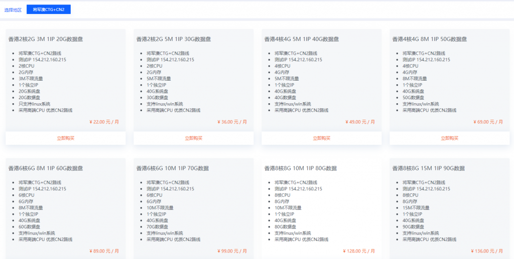
美得云(20元)香港特价将军澳CTG+CN2云服务器
美得云成立于2021年,是一家云产品管理服务商(cloud)专业提供云计算服务、DDOS防护、网络安全服务、国内海外数据中心托管租用等业务、20000+用户的选择,43800+小时稳定运行香港特价将军澳CTG+CN2云服务器、采用高端CPU 优质CN2路线 SDD硬盘。香港CTG+CN22核2G3M20G数据盘25元点击购买香港CTG+CN22核2G5M30G数据盘39元点击购买香港CTG+CN...
pacificrack:2021年七夕VPS特别促销,$13.14/年,2G内存/2核/60gSSD/1T流量,支持Windows
pacificrack官方在搞2021年七夕促销,两款便宜vps给的配置都是挺不错的,依旧是接入1Gbps带宽,KVM虚拟、纯SSD raid10阵列,支持包括Linux、Windows 7、10、server2003、2008、2012、2016、2019在内多种操作系统。本次促销的VPS请特别注意限制条件,见本文末尾!官方网站:https://pacificrack.com支持PayPal、支...

Hostwinds:免费更换IP/优惠码美元VPS免费更换IP4.99,7月最新优惠码西雅图直连VPS
hostwinds怎么样?2021年7月最新 hostwinds 优惠码整理,Hostwinds 优惠套餐整理,Hostwinds 西雅图机房直连线路 VPS 推荐,目前最低仅需 $4.99 月付,并且可以免费更换 IP 地址。本文分享整理一下最新的 Hostwinds 优惠套餐,包括托管型 VPS、无托管型 VPS、Linux VPS、Windows VPS 等多种套餐。目前 Hostwinds...

ncp为你推荐
-
虚机什么是虚拟主机?linux虚拟主机基于linux操作系统的虚拟主机控制面板有哪些?独立ip主机独立IP主机和CDN主机的详细区别?美国vps主机求介绍一款英国的VPS主机?查询ip如何查IP网址免费vps服务器如何免费搭建自己的vps服务器网站空间域名网站、域名空间三者的关系成都虚拟空间五星网络隶属于成都冠一科技有限公司,虚拟空间购买了不到一个月不能访问2次,质量真差啊!网站空间购买购买网站空间需要注意什么虚拟主机管理系统推荐几个适合windows的免费虚拟主机管理系统