Pairwww14dddcom
www14dddcom 时间:2021-04-09 阅读:()
Rev.
1.
04/13Copyright2013bySiliconLaboratoriesSi53156Si53156PCI-EXPRESSGEN1,GEN2,&GEN3FANOUTBUFFERFeaturesApplicationsDescriptionTheSi53156isaspreadtolerablePCIeclockbufferthatcansourcesixPCIeclockssimultaneously.
Thedevicehassixhardwareoutputenablecontrolinputsforenablingtherespectivedifferentialoutputsonthefly.
ThedevicealsofeaturesoutputenablecontrolthroughI2Ccommunication.
I2Cprogrammabilityisalsoavailabletodynamicallycontrolskew,edgerateandamplitudeonthetrue,compliment,orbothdifferentialsignalsontheclockoutputs.
ThiscontrolfeatureenablesoptimalsignalintegrityaswellasoptimalEMIsignatureontheclockoutputs.
FunctionalBlockDiagramPCI-ExpressGen1,Gen2,andGen3compliantSupportsSerialATA(SATA)at100MHz100–210MHzoperationLowpower,pushpull,differentialoutputbuffersInternalterminationformaximumintegrationDedicatedoutputenablepinforeachoutputSixPCI-ExpressbufferedclockoutputsClockinputspreadtolerableSupportsLVDSoutputsI2CsupportwithreadbackcapabilitiesExtendedtemperature:–40to85oC3.
3Vpowersupply32-pinQFNpackageNetworkattachedstorageMulti-functionprintersWirelessaccesspointRoutersControlRAMControl&MemoryDIFFINDIFFINSCLKSDATAOE[5:0]DIFF0DIFF1DIFF2DIFF3DIFF4DIFF5PatentspendingOrderingInformation:Seepage17.
PinAssignmentsVDDOE2*VDDOE3*OE5*OE4*DIFFINDIFFINVDD12345630292827262591011121314242322212019DIFF0DIFF0DIFF1DIFF1VDDDIFF2CKPWRGD_PDB*SDATASCLKVDDDIFF5DIFF5VDDDIFF4DIFF4VDDNC781516DIFF2VDD1817DIFF3DIFF3OE1*OE0*3231*Note:Internal100kohmpull-up.
33GNDSi531562Rev.
1.
0Si53156Rev.
1.
03TABLEOFCONTENTSSectionPage1.
ElectricalSpecifications42.
FunctionalDescription72.
1.
OEPinDefinition72.
2.
OEAssertion72.
3.
OEDeassertion73.
TestandMeasurementSetup84.
ControlRegisters104.
1.
I2CInterface104.
2.
DataProtocol105.
PinDescriptions:32-PinQFN156.
OrderingGuide177.
PackageOutline18ContactInformation20Si531564Rev.
1.
01.
ElectricalSpecificationsTable1.
DCElectricalSpecificationsParameterSymbolTestConditionMinTypMaxUnit3.
3VOperatingVoltageVDDcore3.
3±5%3.
135—3.
465V3.
3VInputHighVoltageVIHControlinputpins2.
0—VDD+0.
3V3.
3VInputLowVoltageVILControlinputpinsVSS–0.
3—0.
8VInputHighVoltageVIHI2CSDATA,SCLK2.
2——VInputLowVoltageVILI2CSDATA,SCLK——1.
0VInputHighLeakageCurrentIIHExceptinternalpull-downresistors,03VOutputHighVoltage(Single-EndedOutputs)VOHIOH=–1mA2.
4——V3.
3VOutputLowVoltage(Single-EndedOutputs)VOLIOL=1mA——0.
4VHigh-impedanceOutputCurrentIOZ–10—10AInputPinCapacitanceCIN1.
5—5pFOutputPinCapacitanceCOUT——6pFPinInductanceLIN——7nHPowerDownCurrentIDD_PD——1mADynamicSupplyCurrentinFanoutModeIDD_3.
3VDifferentialclockswith5"tracesand2pFload,fre-quencyat100MHz——45mASi53156Rev.
1.
05Table2.
ACElectricalSpecificationsParameterSymbolConditionMinTypMaxUnitDIFFINat0.
7VInputFrequencyRangefin100—210MHzRisingandFallingSlewRatesforEachClockOutputSignalinaGivenDifferentialPairTR/TFSingleendedmeasurement:VOL=0.
175toVOH=0.
525V(Averaged)0.
6—4V/nsDifferentialInputHighVoltageVIH150——mVDifferentialInputLowVoltageVIL——–150mVCrossingPointVoltageat0.
7VSwingVOXSingle-endedmeasurement250—550mVVcrossVariationoveralledgesVOXSingle-endedmeasurement——140mVDifferentialRingbackVoltageVRB–100—100mVTimebeforeringbackallowedTSTABLE500——psAbsolutemaximuminputvoltageVMAX——1.
15VAbsoluteminimuminputvoltageVMIN–0.
3——VDutyCycleforEachClockOutputSignalinaGivenDifferentialPairTDCMeasuredatcrossingpointVOX45—55%Rise/FallMatchingTRFMDeterminedasafractionof2x(TR–TF)/(TR+TF)——20%DIFFat0.
7VDutyCycleTDCMeasuredat0Vdifferential45—55%ClockSkewTSKEWMeasuredat0Vdifferential——50psAdditivePeakJitterPk-Pk0—10psAdditivePCIeGen2PhaseJitterRMSGEN210kHz5MHz0—0.
5ps1.
5MHz5psAdditivePCIeGen3PhaseJitterRMSGEN3IncludesPLLBW2–4MHz(CDR=10MHz)0—0.
10psAdditiveCycletoCycleJitterTCCJMeasuredat0Vdifferential——50psLong-termAccuracyLACCMeasuredat0Vdifferential——100ppmRising/FallingSlewrateTR/TFMeasureddifferentiallyfrom±150mV2.
5—8V/nsCrossingPointVoltageat0.
7VSwingVOX300—550mVEnable/DisableandSetupClockStabilizationfromPower-UpTSTABLE–—5msStopclockSet-upTimeTSS10.
0——nsSi531566Rev.
1.
0Table3.
AbsoluteMaximumConditionsParameterSymbolConditionMinTypMaxUnitMainSupplyVoltageVDD_3.
3VFunctional——4.
6VInputVoltageVINRelativetoVSS–0.
5—4.
6VDCTemperature,StorageTSNon-functional–65—150°CIndustrialTemperature,OperatingAmbientTAFunctional–40—85°CCommercialTemperature,OperatingAmbientTAFunctional0—85°CTemperature,JunctionTJFunctional——150°CDissipation,JunctiontoCaseJCJEDEC(JESD51)——17°C/WDissipation,JunctiontoAmbientJAJEDEC(JESD51)——35°C/WESDProtection(HumanBodyModel)ESDHBMJEDEC(JESD22-A114)2000——VFlammabilityRatingUL-94UL(Class)V–0Note:MultipleSupplies:ThevoltageonanyinputorI/Opincannotexceedthepowerpinduringpower-up.
Powersupplysequencingisnotrequired.
Si53156Rev.
1.
072.
FunctionalDescription2.
1.
OEPinDefinitionTheOEpinsareactivehighinputsusedtoenableanddisabletheoutputclocks.
Toenabletheoutputclock,theOEpinneedstobelogichighandtheI2Coutputenablebitneedstobelogichigh.
Therearetwomethodstodisabletheoutputclocks:theOEispulledtoalogiclow,ortheI2Cenablebitissettoalogiclow.
TheOEpinsisrequiredtobedrivenatalltimeandeventhoughithasaninternal100kresistor.
2.
2.
OEAssertionTheOEsignalsareactivehighinputsusedforsynchronousstoppingandstartingtheDIFFoutputclocksrespectivelywhiletherestoftheclockgeneratorcontinuestofunction.
TheassertionoftheOEsignalbymakingitlogichighcausesstoppedrespectiveDIFFoutputstoresumenormaloperation.
Noshortorstretchedclockpulsesareproducedwhentheclockresumes.
Themaximumlatencyfromtheassertiontoactiveoutputsisnomorethantwotosixoutputclockcycles.
2.
3.
OEDeassertionWhentheOEpinisdeassertedbymakingitlogiclow,thecorrespondingDIFFoutputisstopped,andthefinaloutputstateisdrivenlow.
Si531568Rev.
1.
03.
TestandMeasurementSetupThisdiagramshowsthetestloadconfigurationfordifferentialclocksignals.
Figure1.
0.
7VDifferentialLoadConfigurationFigure2.
DifferentialMeasurementforDifferentialOutputSignals(forACParametersMeasurement)Si53156Rev.
1.
09Figure3.
Single-EndedMeasurementforDifferentialOutputSignals(forACParametersMeasurement)Si5315610Rev.
1.
04.
ControlRegisters4.
1.
I2CInterfaceToenhancetheflexibilityandfunctionoftheclockbuffer,anI2Cinterfaceisprovided.
ThroughtheI2CInterface,variousdevicefunctionsareavailable,suchasindividualclockoutputenable.
TheregistersassociatedwiththeI2CInterfaceinitializetotheirdefaultsettingatpower-up.
Theuseofthisinterfaceisoptional.
Clockdeviceregisterchangesarenormallymadeatsysteminitialization,ifanyarerequired.
Powermanagementfunctionscanonlybeprogramedinprogrammodeandnotinnormaloperationmodes.
4.
2.
DataProtocolTheI2Cprotocolacceptsbytewrite,byteread,blockwrite,andblockreadoperationsfromthecontroller.
Forblockwrite/readoperation,accessthebytesinsequentialorderfromlowesttohighest(mostsignificantbitfirst)withtheabilitytostopafteranycompletebyteistransferred.
Forbytewriteandbytereadoperations,thesystemcontrollercanaccessindividuallyindexedbytes.
TheblockwriteandblockreadprotocolisoutlinedinTable4onpage10whileTable5onpage11outlinesbytewriteandbytereadprotocol.
Theslavereceiveraddressis11010110(D6h).
Table4.
BlockReadandBlockWriteProtocolBlockWriteProtocolBlockReadProtocolBitDescriptionBitDescription1Start1Start8:2Slaveaddress—7bits8:2Slaveaddress—7bits9Write9Write10Acknowledgefromslave10Acknowledgefromslave18:11CommandCode—8bits18:11CommandCode–8bits19Acknowledgefromslave19Acknowledgefromslave27:20ByteCount—8bits20Repeatstart28Acknowledgefromslave27:21Slaveaddress—7bits36:29Databyte1–8bits28Read=137Acknowledgefromslave29Acknowledgefromslave45:38Databyte2–8bits37:30ByteCountfromslave—8bits46Acknowledgefromslave38Acknowledge.
.
.
.
DataByte/SlaveAcknowledges46:39Databyte1fromslave—8bits.
.
.
.
DataByteN–8bits47Acknowledge.
.
.
.
Acknowledgefromslave55:48Databyte2fromslave—8bits.
.
.
.
Stop56Acknowledge.
.
.
.
Databytesfromslave/Acknowledge.
.
.
.
DataByteNfromslave—8bits.
.
.
.
NOTAcknowledge.
.
.
.
StopSi53156Rev.
1.
011Table5.
ByteReadandByteWriteProtocolByteWriteProtocolByteReadProtocolBitDescriptionBitDescription1Start1Start8:2Slaveaddress–7bits8:2Slaveaddress–7bits9Write9Write10Acknowledgefromslave10Acknowledgefromslave18:11CommandCode–8bits18:11CommandCode–8bits19Acknowledgefromslave19Acknowledgefromslave27:20Databyte–8bits20Repeatedstart28Acknowledgefromslave27:21Slaveaddress–7bits29Stop28Read29Acknowledgefromslave37:30Datafromslave–8bits38NOTAcknowledge39StopSi5315612Rev.
1.
0Resetsettings=00000000Resetsettings=00010101ControlRegister0.
Byte0BitD7D6D5D4D3D2D1D0NameTypeR/WR/WR/WR/WR/WR/WR/WR/WBitNameFunction7:0ReservedControlRegister1.
Byte1BitD7D6D5D4D3D2D1D0NameDIFF0_OEDIFF1_OEDIFF2_OETypeR/WR/WR/WR/WR/WR/WR/WR/WBitNameFunction7:5Reserved4DIFF0_OEOutputEnableforDIFF0.
0:Outputdisabled.
1:OutputEnabled.
3Reserved2DIFF1_OEOutputEnableforDIFF1.
0:Outputdisabled.
1:Outputenabled.
1Reserved0DIFF2_OEOutputEnableforDIFF2.
0:Outputdisabled.
1:Outputenabled.
Si53156Rev.
1.
013Resetsettings=11100000Resetsettings=00001000ControlRegister2.
Byte2BitD7D6D5D4D3D2D1D0NameDIFF3_OEDIFF4_OEDIFF5_OETypeR/WR/WR/WR/WR/WR/WR/WR/WBitNameFunction7DIFF3_OEOutputEnableforDIFF3.
0:Outputdisabled.
1:Outputenabled.
6DIFF4_OEOutputEnableforDIFF4.
0:Outputdisabled.
1:Outputenabled.
5DIFF5_OEOutputEnableforDIFF5.
0:Outputdisabled.
1:Outputenabled.
4:0ReservedControlRegister3.
Byte3BitD7D6D5D4D3D2D1D0NameRevCode[3:0]VendorID[3:0]TypeR/WR/WR/WR/WR/WR/WR/WR/WBitNameFunction7:4RevCode[3:0]ProgramRevisionCode.
3:0VendorID[3:0]VendorIdentificationCode.
Si5315614Rev.
1.
0Resetsettings=00000110Resetsettings=11011000ControlRegister4.
Byte4BitD7D6D5D4D3D2D1D0NameBC[7:0]TypeR/WR/WR/WR/WR/WR/WR/WR/WBitNameFunction7:0BC[7:0]ByteCountRegister.
ControlRegister5.
Byte5BitD7D6D5D4D3D2D1D0NameDIFF_Amp_SelDIFF_Amp_Cntl[2]DIFF_Amp_Cntl[1]DIFF_Amp_Cntl[0]TypeR/WR/WR/WR/WR/WR/WR/WR/WBitNameFunction7DIFF_Amp_SelAmplitudeControlforDIFFDifferentialOutputs.
0:DifferentialoutputswithDefaultamplitude.
1:DifferentialoutputsamplitudeissetbyByte5[6:4].
6DIFF_Amp_Cntl[2]DIFFDifferentialOutputsAmplitudeAdjustment.
000:300mV001:400mV010:500mV011:600mV100:700mV101:800mV110:900mV111:1000mV5DIFF_Amp_Cntl[1]4DIFF_Amp_Cntl[0]3:0ReservedSi53156Rev.
1.
0155.
PinDescriptions:32-PinQFNFigure4.
32-PinQFNTable6.
Si5315632-PinQFNDescriptionsPin#NameTypeDescription1VDDPWR3.
3Vpowersupply.
2OE2I,PUActivehighinputpinenablesDIFF2(internal100kpull-up).
RefertoTable1onpage4forOEspecifications.
3VDDPWR3.
3VPowerSupply4OE3I,PUActivehighinputpinenablesDIFF3(internal100kpull-up).
RefertoTable1onpage4forOEspecifications.
5OE4I,PUActivehighinputpinenablesDIFF4(internal100kpull-up).
RefertoTable1onpage4forOEspecifications.
6OE5I,PUActivehighinputpinenablesDIFF5(internal100kpull-up).
RefertoTable1onpage4forOEspecifications.
7NCNCNoconnect.
8VDDPWR3.
3Vpowersupply.
9DIFF0O,DIF0.
7V,100MHzdifferentialclock.
10DIFF0O,DIF0.
7V,100MHzdifferentialclock.
11DIFF1O,DIF0.
7V,100MHzdifferentialclock.
VDDOE2*VDDOE3*OE5*OE4*DIFFINDIFFINVDD12345630292827262591011121314242322212019DIFF0DIFF0DIFF1DIFF1VDDDIFF2CKPWRGD_PDB*SDATASCLKVDDDIFF5DIFF5VDDDIFF4DIFF4VDDNC781516DIFF2VDD1817DIFF3DIFF3OE1*OE0*3231*Note:Internal100kohmpull-up.
33GNDSi5315616Rev.
1.
012DIFF1O,DIF0.
7V,100MHzdifferentialclock.
13VDDPWR3.
3Vpowersupply.
14DIFF2O,DIF0.
7V,100MHzdifferentialclock.
15DIFF2O,DIF0.
7V,100MHzdifferentialclock.
16VDDPWR3.
3Vpowersupply.
17DIFF3O,DIF0.
7V,100MHzdifferentialclock.
18DIFF3O,DIF0.
7V,100MHzdifferentialclock.
19DIFF4O,DIF0.
7V,100MHzdifferentialclock.
20DIFF4O,DIF0.
7V,100MHzdifferentialclock.
21VDDPWR3.
3Vpowersupply.
22DIFF5O,DIF0.
7V,100MHzdifferentialclock.
23DIFF5O,DIF0.
7V,100MHzdifferentialclock.
24VDDPWR3.
3Vpowersupply.
25SCLKISMBuscompatibleSCLOCK.
26SDATAI/OSMBuscompatibleSDATA.
27CKPWRGD_PDBI,PU3.
3VLVTTLinput.
Thispinisalevelsensitivestrobeusedtodeterminewhenlatchinputsarevalidandarereadytobesampled.
Areal-timeactivelowinputforassertingpowerdown(PDB)anddisablingalloutputs(internal100kpull-up).
28VDDPWR3.
3Vpowersupply.
29DIFFINI0.
7VDifferentialTrueInput,typically100MHz.
Inputfrequencyrange100to210MHz.
30DIFFINO0.
7VDifferentialComplementInput,typically100MHz.
Inputfrequencyrange100to210MHz.
31OE0I,PUActivehighinputpinenablesDIFF0(internal100kpull-up).
RefertoTable1onpage4forOEspecifications.
32OE1I,PUActivehighinputpinenablesDIFF1(internal100kpull-up).
RefertoTable1onpage4forOEspecifications.
33GNDGNDGroundforbottompadoftheIC.
Table6.
Si5315632-PinQFNDescriptionsPin#NameTypeDescriptionSi53156Rev.
1.
0176.
OrderingGuidePartNumberPackageTypeTemperatureLead-freeSi53156-A01AGM32-pinQFNExtended,–40to85CSi53156-A01AGMR32-pinQFN—TapeandReelExtended,–40to85CSi5315618Rev.
1.
07.
PackageOutlineFigure5illustratesthepackagedetailsfortheSi53156.
Table7liststhevaluesforthedimensionsshownintheillustration.
Figure5.
32-PinQuadFlatNoLead(QFN)PackageTable7.
PackageDiagramDimensionsDimensionMinNomMaxA0.
700.
750.
80A10.
000.
020.
05b0.
180.
250.
30D5.
00BSCD23.
153.
203.
25e0.
50BSCE5.
00BSCE23.
153.
203.
25L0.
300.
400.
50aaa0.
10bbb0.
10ccc0.
08ddd0.
10Notes:1.
Alldimensionsshownareinmillimeters(mm)unlessotherwisenoted.
2.
DimensioningandTolerancingperANSIY14.
5M-1994.
3.
RecommendedcardreflowprofileispertheJEDEC/IPCJ-STD-020specificationforSmallBodyComponents.
4.
Coplanaritylessthan0.
08mm.
5.
Terminal#1identifierandterminalnumberingconventionconformtoJESD95-1SPP-012.
Si53156Rev.
1.
019DOCUMENTCHANGELISTRevision0.
1toRevision1.
0UpdatedFeaturesandDescription.
UpdatedTable2.
UpdatedTable3.
UpdatedSection4.
1.
Si5315620Rev.
1.
0CONTACTINFORMATIONSiliconLaboratoriesInc.
400WestCesarChavezAustin,TX78701Tel:1+(512)416-8500Fax:1+(512)416-9669TollFree:1+(877)444-3032PleasevisittheSiliconLabsTechnicalSupportwebpage:https://www.
silabs.
com/support/pages/contacttechnicalsupport.
aspxandregistertosubmitatechnicalsupportrequest.
PatentNoticeSiliconLabsinvestsinresearchanddevelopmenttohelpourcustomersdifferentiateinthemarketwithinnovativelow-power,smallsize,analog-intensivemixed-signalsolutions.
SiliconLabs'extensivepatentportfolioisatestamenttoouruniqueapproachandworld-classengineeringteam.
SiliconLaboratoriesandSiliconLabsaretrademarksofSiliconLaboratoriesInc.
Otherproductsorbrandnamesmentionedhereinaretrademarksorregisteredtrademarksoftheirrespectiveholders.
Theinformationinthisdocumentisbelievedtobeaccurateinallrespectsatthetimeofpublicationbutissubjecttochangewithoutnotice.
SiliconLaboratoriesassumesnoresponsibilityforerrorsandomissions,anddisclaimsresponsibilityforanyconsequencesresultingfromtheuseofinformationincludedherein.
Additionally,SiliconLaboratoriesassumesnoresponsibilityforthefunctioningofundescribedfea-turesorparameters.
SiliconLaboratoriesreservestherighttomakechangeswithoutfurthernotice.
SiliconLaboratoriesmakesnowarran-ty,representationorguaranteeregardingthesuitabilityofitsproductsforanyparticularpurpose,nordoesSiliconLaboratoriesassumeanyliabilityarisingoutoftheapplicationoruseofanyproductorcircuit,andspecificallydisclaimsanyandallliability,includingwithoutlimitationconsequentialorincidentaldamages.
SiliconLaboratoriesproductsarenotdesigned,intended,orauthorizedforuseinapplicationsintend-edtosupportorsustainlife,orforanyotherapplicationinwhichthefailureoftheSiliconLaboratoriesproductcouldcreateasituationwherepersonalinjuryordeathmayoccur.
ShouldBuyerpurchaseoruseSiliconLaboratoriesproductsforanysuchunintendedorunauthorizedapplication,BuyershallindemnifyandholdSiliconLaboratoriesharmlessagainstallclaimsanddamages.
1.
04/13Copyright2013bySiliconLaboratoriesSi53156Si53156PCI-EXPRESSGEN1,GEN2,&GEN3FANOUTBUFFERFeaturesApplicationsDescriptionTheSi53156isaspreadtolerablePCIeclockbufferthatcansourcesixPCIeclockssimultaneously.
Thedevicehassixhardwareoutputenablecontrolinputsforenablingtherespectivedifferentialoutputsonthefly.
ThedevicealsofeaturesoutputenablecontrolthroughI2Ccommunication.
I2Cprogrammabilityisalsoavailabletodynamicallycontrolskew,edgerateandamplitudeonthetrue,compliment,orbothdifferentialsignalsontheclockoutputs.
ThiscontrolfeatureenablesoptimalsignalintegrityaswellasoptimalEMIsignatureontheclockoutputs.
FunctionalBlockDiagramPCI-ExpressGen1,Gen2,andGen3compliantSupportsSerialATA(SATA)at100MHz100–210MHzoperationLowpower,pushpull,differentialoutputbuffersInternalterminationformaximumintegrationDedicatedoutputenablepinforeachoutputSixPCI-ExpressbufferedclockoutputsClockinputspreadtolerableSupportsLVDSoutputsI2CsupportwithreadbackcapabilitiesExtendedtemperature:–40to85oC3.
3Vpowersupply32-pinQFNpackageNetworkattachedstorageMulti-functionprintersWirelessaccesspointRoutersControlRAMControl&MemoryDIFFINDIFFINSCLKSDATAOE[5:0]DIFF0DIFF1DIFF2DIFF3DIFF4DIFF5PatentspendingOrderingInformation:Seepage17.
PinAssignmentsVDDOE2*VDDOE3*OE5*OE4*DIFFINDIFFINVDD12345630292827262591011121314242322212019DIFF0DIFF0DIFF1DIFF1VDDDIFF2CKPWRGD_PDB*SDATASCLKVDDDIFF5DIFF5VDDDIFF4DIFF4VDDNC781516DIFF2VDD1817DIFF3DIFF3OE1*OE0*3231*Note:Internal100kohmpull-up.
33GNDSi531562Rev.
1.
0Si53156Rev.
1.
03TABLEOFCONTENTSSectionPage1.
ElectricalSpecifications42.
FunctionalDescription72.
1.
OEPinDefinition72.
2.
OEAssertion72.
3.
OEDeassertion73.
TestandMeasurementSetup84.
ControlRegisters104.
1.
I2CInterface104.
2.
DataProtocol105.
PinDescriptions:32-PinQFN156.
OrderingGuide177.
PackageOutline18ContactInformation20Si531564Rev.
1.
01.
ElectricalSpecificationsTable1.
DCElectricalSpecificationsParameterSymbolTestConditionMinTypMaxUnit3.
3VOperatingVoltageVDDcore3.
3±5%3.
135—3.
465V3.
3VInputHighVoltageVIHControlinputpins2.
0—VDD+0.
3V3.
3VInputLowVoltageVILControlinputpinsVSS–0.
3—0.
8VInputHighVoltageVIHI2CSDATA,SCLK2.
2——VInputLowVoltageVILI2CSDATA,SCLK——1.
0VInputHighLeakageCurrentIIHExceptinternalpull-downresistors,0
4——V3.
3VOutputLowVoltage(Single-EndedOutputs)VOLIOL=1mA——0.
4VHigh-impedanceOutputCurrentIOZ–10—10AInputPinCapacitanceCIN1.
5—5pFOutputPinCapacitanceCOUT——6pFPinInductanceLIN——7nHPowerDownCurrentIDD_PD——1mADynamicSupplyCurrentinFanoutModeIDD_3.
3VDifferentialclockswith5"tracesand2pFload,fre-quencyat100MHz——45mASi53156Rev.
1.
05Table2.
ACElectricalSpecificationsParameterSymbolConditionMinTypMaxUnitDIFFINat0.
7VInputFrequencyRangefin100—210MHzRisingandFallingSlewRatesforEachClockOutputSignalinaGivenDifferentialPairTR/TFSingleendedmeasurement:VOL=0.
175toVOH=0.
525V(Averaged)0.
6—4V/nsDifferentialInputHighVoltageVIH150——mVDifferentialInputLowVoltageVIL——–150mVCrossingPointVoltageat0.
7VSwingVOXSingle-endedmeasurement250—550mVVcrossVariationoveralledgesVOXSingle-endedmeasurement——140mVDifferentialRingbackVoltageVRB–100—100mVTimebeforeringbackallowedTSTABLE500——psAbsolutemaximuminputvoltageVMAX——1.
15VAbsoluteminimuminputvoltageVMIN–0.
3——VDutyCycleforEachClockOutputSignalinaGivenDifferentialPairTDCMeasuredatcrossingpointVOX45—55%Rise/FallMatchingTRFMDeterminedasafractionof2x(TR–TF)/(TR+TF)——20%DIFFat0.
7VDutyCycleTDCMeasuredat0Vdifferential45—55%ClockSkewTSKEWMeasuredat0Vdifferential——50psAdditivePeakJitterPk-Pk0—10psAdditivePCIeGen2PhaseJitterRMSGEN210kHz
5ps1.
5MHz
10psAdditiveCycletoCycleJitterTCCJMeasuredat0Vdifferential——50psLong-termAccuracyLACCMeasuredat0Vdifferential——100ppmRising/FallingSlewrateTR/TFMeasureddifferentiallyfrom±150mV2.
5—8V/nsCrossingPointVoltageat0.
7VSwingVOX300—550mVEnable/DisableandSetupClockStabilizationfromPower-UpTSTABLE–—5msStopclockSet-upTimeTSS10.
0——nsSi531566Rev.
1.
0Table3.
AbsoluteMaximumConditionsParameterSymbolConditionMinTypMaxUnitMainSupplyVoltageVDD_3.
3VFunctional——4.
6VInputVoltageVINRelativetoVSS–0.
5—4.
6VDCTemperature,StorageTSNon-functional–65—150°CIndustrialTemperature,OperatingAmbientTAFunctional–40—85°CCommercialTemperature,OperatingAmbientTAFunctional0—85°CTemperature,JunctionTJFunctional——150°CDissipation,JunctiontoCaseJCJEDEC(JESD51)——17°C/WDissipation,JunctiontoAmbientJAJEDEC(JESD51)——35°C/WESDProtection(HumanBodyModel)ESDHBMJEDEC(JESD22-A114)2000——VFlammabilityRatingUL-94UL(Class)V–0Note:MultipleSupplies:ThevoltageonanyinputorI/Opincannotexceedthepowerpinduringpower-up.
Powersupplysequencingisnotrequired.
Si53156Rev.
1.
072.
FunctionalDescription2.
1.
OEPinDefinitionTheOEpinsareactivehighinputsusedtoenableanddisabletheoutputclocks.
Toenabletheoutputclock,theOEpinneedstobelogichighandtheI2Coutputenablebitneedstobelogichigh.
Therearetwomethodstodisabletheoutputclocks:theOEispulledtoalogiclow,ortheI2Cenablebitissettoalogiclow.
TheOEpinsisrequiredtobedrivenatalltimeandeventhoughithasaninternal100kresistor.
2.
2.
OEAssertionTheOEsignalsareactivehighinputsusedforsynchronousstoppingandstartingtheDIFFoutputclocksrespectivelywhiletherestoftheclockgeneratorcontinuestofunction.
TheassertionoftheOEsignalbymakingitlogichighcausesstoppedrespectiveDIFFoutputstoresumenormaloperation.
Noshortorstretchedclockpulsesareproducedwhentheclockresumes.
Themaximumlatencyfromtheassertiontoactiveoutputsisnomorethantwotosixoutputclockcycles.
2.
3.
OEDeassertionWhentheOEpinisdeassertedbymakingitlogiclow,thecorrespondingDIFFoutputisstopped,andthefinaloutputstateisdrivenlow.
Si531568Rev.
1.
03.
TestandMeasurementSetupThisdiagramshowsthetestloadconfigurationfordifferentialclocksignals.
Figure1.
0.
7VDifferentialLoadConfigurationFigure2.
DifferentialMeasurementforDifferentialOutputSignals(forACParametersMeasurement)Si53156Rev.
1.
09Figure3.
Single-EndedMeasurementforDifferentialOutputSignals(forACParametersMeasurement)Si5315610Rev.
1.
04.
ControlRegisters4.
1.
I2CInterfaceToenhancetheflexibilityandfunctionoftheclockbuffer,anI2Cinterfaceisprovided.
ThroughtheI2CInterface,variousdevicefunctionsareavailable,suchasindividualclockoutputenable.
TheregistersassociatedwiththeI2CInterfaceinitializetotheirdefaultsettingatpower-up.
Theuseofthisinterfaceisoptional.
Clockdeviceregisterchangesarenormallymadeatsysteminitialization,ifanyarerequired.
Powermanagementfunctionscanonlybeprogramedinprogrammodeandnotinnormaloperationmodes.
4.
2.
DataProtocolTheI2Cprotocolacceptsbytewrite,byteread,blockwrite,andblockreadoperationsfromthecontroller.
Forblockwrite/readoperation,accessthebytesinsequentialorderfromlowesttohighest(mostsignificantbitfirst)withtheabilitytostopafteranycompletebyteistransferred.
Forbytewriteandbytereadoperations,thesystemcontrollercanaccessindividuallyindexedbytes.
TheblockwriteandblockreadprotocolisoutlinedinTable4onpage10whileTable5onpage11outlinesbytewriteandbytereadprotocol.
Theslavereceiveraddressis11010110(D6h).
Table4.
BlockReadandBlockWriteProtocolBlockWriteProtocolBlockReadProtocolBitDescriptionBitDescription1Start1Start8:2Slaveaddress—7bits8:2Slaveaddress—7bits9Write9Write10Acknowledgefromslave10Acknowledgefromslave18:11CommandCode—8bits18:11CommandCode–8bits19Acknowledgefromslave19Acknowledgefromslave27:20ByteCount—8bits20Repeatstart28Acknowledgefromslave27:21Slaveaddress—7bits36:29Databyte1–8bits28Read=137Acknowledgefromslave29Acknowledgefromslave45:38Databyte2–8bits37:30ByteCountfromslave—8bits46Acknowledgefromslave38Acknowledge.
.
.
.
DataByte/SlaveAcknowledges46:39Databyte1fromslave—8bits.
.
.
.
DataByteN–8bits47Acknowledge.
.
.
.
Acknowledgefromslave55:48Databyte2fromslave—8bits.
.
.
.
Stop56Acknowledge.
.
.
.
Databytesfromslave/Acknowledge.
.
.
.
DataByteNfromslave—8bits.
.
.
.
NOTAcknowledge.
.
.
.
StopSi53156Rev.
1.
011Table5.
ByteReadandByteWriteProtocolByteWriteProtocolByteReadProtocolBitDescriptionBitDescription1Start1Start8:2Slaveaddress–7bits8:2Slaveaddress–7bits9Write9Write10Acknowledgefromslave10Acknowledgefromslave18:11CommandCode–8bits18:11CommandCode–8bits19Acknowledgefromslave19Acknowledgefromslave27:20Databyte–8bits20Repeatedstart28Acknowledgefromslave27:21Slaveaddress–7bits29Stop28Read29Acknowledgefromslave37:30Datafromslave–8bits38NOTAcknowledge39StopSi5315612Rev.
1.
0Resetsettings=00000000Resetsettings=00010101ControlRegister0.
Byte0BitD7D6D5D4D3D2D1D0NameTypeR/WR/WR/WR/WR/WR/WR/WR/WBitNameFunction7:0ReservedControlRegister1.
Byte1BitD7D6D5D4D3D2D1D0NameDIFF0_OEDIFF1_OEDIFF2_OETypeR/WR/WR/WR/WR/WR/WR/WR/WBitNameFunction7:5Reserved4DIFF0_OEOutputEnableforDIFF0.
0:Outputdisabled.
1:OutputEnabled.
3Reserved2DIFF1_OEOutputEnableforDIFF1.
0:Outputdisabled.
1:Outputenabled.
1Reserved0DIFF2_OEOutputEnableforDIFF2.
0:Outputdisabled.
1:Outputenabled.
Si53156Rev.
1.
013Resetsettings=11100000Resetsettings=00001000ControlRegister2.
Byte2BitD7D6D5D4D3D2D1D0NameDIFF3_OEDIFF4_OEDIFF5_OETypeR/WR/WR/WR/WR/WR/WR/WR/WBitNameFunction7DIFF3_OEOutputEnableforDIFF3.
0:Outputdisabled.
1:Outputenabled.
6DIFF4_OEOutputEnableforDIFF4.
0:Outputdisabled.
1:Outputenabled.
5DIFF5_OEOutputEnableforDIFF5.
0:Outputdisabled.
1:Outputenabled.
4:0ReservedControlRegister3.
Byte3BitD7D6D5D4D3D2D1D0NameRevCode[3:0]VendorID[3:0]TypeR/WR/WR/WR/WR/WR/WR/WR/WBitNameFunction7:4RevCode[3:0]ProgramRevisionCode.
3:0VendorID[3:0]VendorIdentificationCode.
Si5315614Rev.
1.
0Resetsettings=00000110Resetsettings=11011000ControlRegister4.
Byte4BitD7D6D5D4D3D2D1D0NameBC[7:0]TypeR/WR/WR/WR/WR/WR/WR/WR/WBitNameFunction7:0BC[7:0]ByteCountRegister.
ControlRegister5.
Byte5BitD7D6D5D4D3D2D1D0NameDIFF_Amp_SelDIFF_Amp_Cntl[2]DIFF_Amp_Cntl[1]DIFF_Amp_Cntl[0]TypeR/WR/WR/WR/WR/WR/WR/WR/WBitNameFunction7DIFF_Amp_SelAmplitudeControlforDIFFDifferentialOutputs.
0:DifferentialoutputswithDefaultamplitude.
1:DifferentialoutputsamplitudeissetbyByte5[6:4].
6DIFF_Amp_Cntl[2]DIFFDifferentialOutputsAmplitudeAdjustment.
000:300mV001:400mV010:500mV011:600mV100:700mV101:800mV110:900mV111:1000mV5DIFF_Amp_Cntl[1]4DIFF_Amp_Cntl[0]3:0ReservedSi53156Rev.
1.
0155.
PinDescriptions:32-PinQFNFigure4.
32-PinQFNTable6.
Si5315632-PinQFNDescriptionsPin#NameTypeDescription1VDDPWR3.
3Vpowersupply.
2OE2I,PUActivehighinputpinenablesDIFF2(internal100kpull-up).
RefertoTable1onpage4forOEspecifications.
3VDDPWR3.
3VPowerSupply4OE3I,PUActivehighinputpinenablesDIFF3(internal100kpull-up).
RefertoTable1onpage4forOEspecifications.
5OE4I,PUActivehighinputpinenablesDIFF4(internal100kpull-up).
RefertoTable1onpage4forOEspecifications.
6OE5I,PUActivehighinputpinenablesDIFF5(internal100kpull-up).
RefertoTable1onpage4forOEspecifications.
7NCNCNoconnect.
8VDDPWR3.
3Vpowersupply.
9DIFF0O,DIF0.
7V,100MHzdifferentialclock.
10DIFF0O,DIF0.
7V,100MHzdifferentialclock.
11DIFF1O,DIF0.
7V,100MHzdifferentialclock.
VDDOE2*VDDOE3*OE5*OE4*DIFFINDIFFINVDD12345630292827262591011121314242322212019DIFF0DIFF0DIFF1DIFF1VDDDIFF2CKPWRGD_PDB*SDATASCLKVDDDIFF5DIFF5VDDDIFF4DIFF4VDDNC781516DIFF2VDD1817DIFF3DIFF3OE1*OE0*3231*Note:Internal100kohmpull-up.
33GNDSi5315616Rev.
1.
012DIFF1O,DIF0.
7V,100MHzdifferentialclock.
13VDDPWR3.
3Vpowersupply.
14DIFF2O,DIF0.
7V,100MHzdifferentialclock.
15DIFF2O,DIF0.
7V,100MHzdifferentialclock.
16VDDPWR3.
3Vpowersupply.
17DIFF3O,DIF0.
7V,100MHzdifferentialclock.
18DIFF3O,DIF0.
7V,100MHzdifferentialclock.
19DIFF4O,DIF0.
7V,100MHzdifferentialclock.
20DIFF4O,DIF0.
7V,100MHzdifferentialclock.
21VDDPWR3.
3Vpowersupply.
22DIFF5O,DIF0.
7V,100MHzdifferentialclock.
23DIFF5O,DIF0.
7V,100MHzdifferentialclock.
24VDDPWR3.
3Vpowersupply.
25SCLKISMBuscompatibleSCLOCK.
26SDATAI/OSMBuscompatibleSDATA.
27CKPWRGD_PDBI,PU3.
3VLVTTLinput.
Thispinisalevelsensitivestrobeusedtodeterminewhenlatchinputsarevalidandarereadytobesampled.
Areal-timeactivelowinputforassertingpowerdown(PDB)anddisablingalloutputs(internal100kpull-up).
28VDDPWR3.
3Vpowersupply.
29DIFFINI0.
7VDifferentialTrueInput,typically100MHz.
Inputfrequencyrange100to210MHz.
30DIFFINO0.
7VDifferentialComplementInput,typically100MHz.
Inputfrequencyrange100to210MHz.
31OE0I,PUActivehighinputpinenablesDIFF0(internal100kpull-up).
RefertoTable1onpage4forOEspecifications.
32OE1I,PUActivehighinputpinenablesDIFF1(internal100kpull-up).
RefertoTable1onpage4forOEspecifications.
33GNDGNDGroundforbottompadoftheIC.
Table6.
Si5315632-PinQFNDescriptionsPin#NameTypeDescriptionSi53156Rev.
1.
0176.
OrderingGuidePartNumberPackageTypeTemperatureLead-freeSi53156-A01AGM32-pinQFNExtended,–40to85CSi53156-A01AGMR32-pinQFN—TapeandReelExtended,–40to85CSi5315618Rev.
1.
07.
PackageOutlineFigure5illustratesthepackagedetailsfortheSi53156.
Table7liststhevaluesforthedimensionsshownintheillustration.
Figure5.
32-PinQuadFlatNoLead(QFN)PackageTable7.
PackageDiagramDimensionsDimensionMinNomMaxA0.
700.
750.
80A10.
000.
020.
05b0.
180.
250.
30D5.
00BSCD23.
153.
203.
25e0.
50BSCE5.
00BSCE23.
153.
203.
25L0.
300.
400.
50aaa0.
10bbb0.
10ccc0.
08ddd0.
10Notes:1.
Alldimensionsshownareinmillimeters(mm)unlessotherwisenoted.
2.
DimensioningandTolerancingperANSIY14.
5M-1994.
3.
RecommendedcardreflowprofileispertheJEDEC/IPCJ-STD-020specificationforSmallBodyComponents.
4.
Coplanaritylessthan0.
08mm.
5.
Terminal#1identifierandterminalnumberingconventionconformtoJESD95-1SPP-012.
Si53156Rev.
1.
019DOCUMENTCHANGELISTRevision0.
1toRevision1.
0UpdatedFeaturesandDescription.
UpdatedTable2.
UpdatedTable3.
UpdatedSection4.
1.
Si5315620Rev.
1.
0CONTACTINFORMATIONSiliconLaboratoriesInc.
400WestCesarChavezAustin,TX78701Tel:1+(512)416-8500Fax:1+(512)416-9669TollFree:1+(877)444-3032PleasevisittheSiliconLabsTechnicalSupportwebpage:https://www.
silabs.
com/support/pages/contacttechnicalsupport.
aspxandregistertosubmitatechnicalsupportrequest.
PatentNoticeSiliconLabsinvestsinresearchanddevelopmenttohelpourcustomersdifferentiateinthemarketwithinnovativelow-power,smallsize,analog-intensivemixed-signalsolutions.
SiliconLabs'extensivepatentportfolioisatestamenttoouruniqueapproachandworld-classengineeringteam.
SiliconLaboratoriesandSiliconLabsaretrademarksofSiliconLaboratoriesInc.
Otherproductsorbrandnamesmentionedhereinaretrademarksorregisteredtrademarksoftheirrespectiveholders.
Theinformationinthisdocumentisbelievedtobeaccurateinallrespectsatthetimeofpublicationbutissubjecttochangewithoutnotice.
SiliconLaboratoriesassumesnoresponsibilityforerrorsandomissions,anddisclaimsresponsibilityforanyconsequencesresultingfromtheuseofinformationincludedherein.
Additionally,SiliconLaboratoriesassumesnoresponsibilityforthefunctioningofundescribedfea-turesorparameters.
SiliconLaboratoriesreservestherighttomakechangeswithoutfurthernotice.
SiliconLaboratoriesmakesnowarran-ty,representationorguaranteeregardingthesuitabilityofitsproductsforanyparticularpurpose,nordoesSiliconLaboratoriesassumeanyliabilityarisingoutoftheapplicationoruseofanyproductorcircuit,andspecificallydisclaimsanyandallliability,includingwithoutlimitationconsequentialorincidentaldamages.
SiliconLaboratoriesproductsarenotdesigned,intended,orauthorizedforuseinapplicationsintend-edtosupportorsustainlife,orforanyotherapplicationinwhichthefailureoftheSiliconLaboratoriesproductcouldcreateasituationwherepersonalinjuryordeathmayoccur.
ShouldBuyerpurchaseoruseSiliconLaboratoriesproductsforanysuchunintendedorunauthorizedapplication,BuyershallindemnifyandholdSiliconLaboratoriesharmlessagainstallclaimsanddamages.
- Pairwww14dddcom相关文档
- 充电www14dddcom
- 2015.www14dddcom
- www14dddcom14ddd为什么打不开
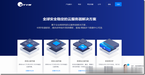
DiyVM:499元/月香港沙田服务器,L5630*2/16G内存/120G SSD硬盘/5M CN2线路
DiyVM是一家成立于2009年的国人主机商,提供的产品包括VPS主机、独立服务器租用等,产品数据中心包括中国香港、日本大阪和美国洛杉矶等,其中VPS主机基于XEN架构,支持异地备份与自定义镜像,VPS和独立服务器均可提供内网IP功能。商家VPS主机均2GB内存起步,三个地区机房可选,使用优惠码后每月69元起;独立服务器开设在香港沙田电信机房,CN2线路,自动化开通上架,最低499元/月起。下面以...
pacificrack7月美国便宜支持win VPS,$19.99/年,2G内存/1核/50gSSD/1T流量
pacificrack发布了7月最新vps优惠,新款促销便宜vps采用的是魔方管理,也就是PR-M系列。提一下有意思的是这次支持Windows server 2003、2008R2、2012R2、2016、2019、Windows 7、Windows 10,当然啦,常规Linux系统是必不可少的!1Gbps带宽、KVM虚拟、纯SSD raid10、自家QN机房洛杉矶数据中心...支持PayPal、...

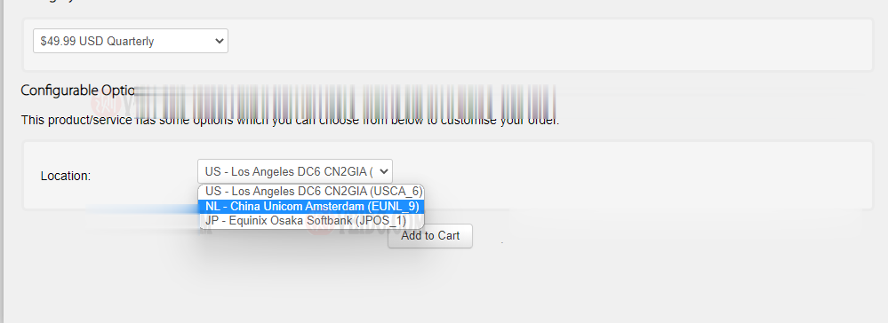
搬瓦工:新增荷兰机房 EUNL_9 测评,联通 AS10099/AS9929 高端优化路线/速度 延迟 路由 丢包测试
搬瓦工最近上线了一个新的荷兰机房,荷兰 EUNL_9 机房,这个 9 的编号感觉也挺随性的,之前的荷兰机房编号是 EUNL_3。这次荷兰新机房 EUNL_9 采用联通 AS9929 高端路线,三网都接入了 AS9929,对于联通用户来说是个好消息,又多了一个选择。对于其他用户可能还是 CN2 GIA 机房更合适一些。其实对于联通用户,这个荷兰机房也是比较远的,相比之下日本软银 JPOS_1 机房可...
www14dddcom为你推荐
-
johncusack有喜欢演员JOHN CUSACK的吗?从哪部片子开始喜欢他的?至今为止他主要参与的电影作品有哪些?psbc.com怎样登录wap.psbc.com冯媛甑冯媛甄多大啊?百花百游百花净斑方多少钱一盒同一ip网站同IP的网站互相链接会被K吗?avtt4.comwww.51kao4.com为什么进不去啊?www.5any.com重庆哪里有不是全日制的大学?javbibitreebibi是什么牌子的杨丽晓博客杨丽晓哪一年出生的?ename.com要怎么在Ename.cn上注册个人域名?