Outputdellt110
dellt110 时间:2021-03-26 阅读:()
SemiconductorComponentsIndustries,LLC,2017October,2017Rev.
P51PublicationOrderNumber:NCP110/DNCP110ProductPreview200mA,LowVIN,LowNoiseandHighPSRRLDORegulatorTheNCP110isalinearregulatorcapableofsupplying200mAoutputcurrentfrom1.
1Vinputvoltage.
Thedeviceprovideswideoutputrangefrom0.
6Vupto4.
0V,verylownoiseandhighPSRR.
DuetolowquiescentcurrenttheNCP110issuitableforbatterypowereddevicessuchassmartphonesandtablets.
Thedeviceisdesignedtoworkwitha1mFinputanda1mFoutputceramiccapacitor.
Itisavailableinultrasmall0.
35P,0.
65mmx0.
65mmChipScalePackage(CSP)andXDFN40.
65P,1mmx1mm.
FeaturesOperatingInputVoltageRange:1.
1Vto5.
5VAvailableinFixedVoltageOption:0.
6Vto4.
0V±2%AccuracyOverLoad/TemperatureUltraLowQuiescentCurrentTyp.
18mAStandbyCurrent:Typ.
0.
1mAVeryLowDropout:70mVfor1.
05V@100mAHighPSRR:Typ.
95dBat20mA,f=1kHzUltraLowNoise:8.
8mVRMSStablewitha1mFSmallCaseSizeCeramicCapacitorsAvailableinWLCSP40.
65mmx0.
65mmx0.
33mmCase567JZXDFN41mmx1mmx0.
4mmCase711AJTheseDevicesarePbFree,HalogenFree/BFRFreeandareRoHSCompliantTypicalApplicationsBatterypoweredEquipmentWirelessLANDevicesSmartphones,TabletsCameras,DVRs,STBandCamcordersINENGNDOUTOFFONFigure1.
TypicalApplicationSchematicsVOUTCOUT1mFCeramicVINNCP110CIN1mFCeramicThisdocumentcontainsinformationonaproductunderdevelopment.
ONSemiconductorreservestherighttochangeordiscontinuethisproductwithoutnotice.
MARKINGDIAGRAMSwww.
onsemi.
comXorXX=SpecificDeviceCodeM=DateCodeSeedetailedordering,markingandshippinginformationonpage4ofthisdatasheet.
ORDERINGINFORMATIONPINCONNECTIONSXDFN4CASE711AJA1A2B1B2INOUTENGND(TopView)(TopView)WLCSP4CASE567JZA1X1XXM1NCP110www.
onsemi.
com2Figure2.
SimplifiedSchematicBlockDiagramINTHERMALSHUTDOWNMOSFETDRIVERWITHCURRENTLIMITINTEGRATEDSOFTSTARTBANDGAPREFERENCEENABLELOGICENOUTGNDEN*ActiveDischargeOnlyPINFUNCTIONDESCRIPTIONPinNo.
CSP4PinNo.
XDFN4PinNameDescriptionA14INInputvoltagesupplypinA21OUTRegulatedoutputvoltage.
Theoutputshouldbebypassedwithsmall1mFceramiccapacitor.
B13ENChipenable:ApplyingVEN0.
7VenablestheLDO.
B22GNDCommongroundconnectionEPADEPADExposepadcanbetiedtogroundplaneforbetterpowerdissipationABSOLUTEMAXIMUMRATINGSRatingSymbolValueUnitInputVoltage(Note1)VIN0.
3Vto6VOutputVoltageVOUT0.
3toVIN+0.
3,max.
6VVChipEnableInputVCE0.
3toVIN+0.
3,max.
6VVOutputShortCircuitDurationtSCunlimitedsMaximumJunctionTemperatureTJ150°CStorageTemperatureTSTG55to150°CESDCapability,HumanBodyModel(Note2)ESDHBM2000VESDCapability,MachineModel(Note2)ESDMM200VStressesexceedingthoselistedintheMaximumRatingstablemaydamagethedevice.
Ifanyoftheselimitsareexceeded,devicefunctionalityshouldnotbeassumed,damagemayoccurandreliabilitymaybeaffected.
1.
RefertoELECTRICALCHARACTERISTICSandAPPLICATIONINFORMATIONforSafeOperatingArea.
2.
ThisdeviceseriesincorporatesESDprotectionandistestedbythefollowingmethods:ESDHumanBodyModeltestedperEIA/JESD22A114ESDMachineModeltestedperEIA/JESD22A115LatchupCurrentMaximumRatingtestedperJEDECstandard:JESD78.
THERMALCHARACTERISTICSRatingSymbolValueUnitThermalCharacteristics,CSP4(Note3)ThermalResistance,JunctiontoAirRqJA108°C/WThermalCharacteristics,XDFN4(Note3)ThermalResistance,JunctiontoAir198.
13.
MeasuredaccordingtoJEDECboardspecification.
DetaileddescriptionoftheboardcanbefoundinJESD517NCP110www.
onsemi.
com3ELECTRICALCHARACTERISTICS40°C≤TJ≤125°C;VIN=VOUT(NOM)+0.
3Vor1.
1V,whicheverisgreater;IOUT=1mA,CIN=COUT=1mF,unlessotherwisenoted.
VEN=1.
0V.
TypicalvaluesareatTJ=+25°C(Note4).
ParameterTestConditionsSymbolMinTypMaxUnitOperatingInputVoltageVIN1.
15.
5VOutputVoltageAccuracyVIN=VOUT(NOM)+0.
3V(VIN≥1.
1V)VOUT(NOM)≤1.
5VVOUT30+30mVVOUT(NOM)>1.
5V2+2%LineRegulationVOUT(NOM)+0.
5V≤VIN≤5.
5V,(VIN≥1.
1V)LineReg0.
02%/VLoadRegulationIOUT=1mAto200mALoadReg0.
001%/mADropoutVoltage(Note5)VOUT(NOM)=1.
05VIOUT=50mAVDO4070mVIOUT=100mA70130VOUT(NOM)=1.
20VIOUT=110mA60140IOUT=200mA110190OutputCurrentLimitVOUT=90%VOUT(NOM)ICL225300mAShortCircuitCurrentVOUT=0VISC300QuiescentCurrentIOUT=0mAIQ2025mAShutdownCurrentVEN≤0.
2V,VIN=1.
1VIDIS0.
011.
0mAENPinThresholdVoltageENInputVoltage"H"VENH0.
7VENInputVoltage"L"VENL0.
2ENPullDownCurrentVEN=1.
1VIEN0.
20.
5mATurnOnTimeCOUT=1mF,FromassertionofVENtoVOUT=95%VOUT(NOM)tON120msPowerSupplyRejectionRatioIOUT=20mA,VIN=VOUT+0.
3Vf=100Hzf=1kHzf=10kHzf=100kHzPSRR90958555dBOutputVoltageNoisef=10Hzto100kHzVN8.
8mVRMSThermalShutdownThresholdTemperaturerisingTSDH160°CTemperaturefallingTSDL140°CActiveOutputDischargeResis-tanceVEN<0.
2V,VersionAonlyRDIS280WProductparametricperformanceisindicatedintheElectricalCharacteristicsforthelistedtestconditions,unlessotherwisenoted.
ProductperformancemaynotbeindicatedbytheElectricalCharacteristicsifoperatedunderdifferentconditions.
4.
Performanceguaranteedovertheindicatedoperatingtemperaturerangebydesignand/orcharacterization.
ProductiontestedatTA=25°C.
Lowdutycyclepulsetechniquesareusedduringthetestingtomaintainthejunctiontemperatureasclosetoambientaspossible.
5.
DropoutvoltageischaracterizedwhenVOUTfalls0.
02xVOUT(NOM)belowVOUT(NOM).
6.
Guaranteedbydesign.
NCP110www.
onsemi.
com4ORDERINGINFORMATIONDeviceNominalOutputVoltageMarkingDescriptionRotationPackageShippingNCP110AFCT060T2G0.
60VC200mA,ActiveDischarge0°WLCSP4CASE567JZ(Pb-Free)5000/Tape&ReelNCP110AFCT105T2G1.
05VA0°NCP110AFCT120T2G1.
20VF0°NCP110AFCT180T2G1.
80VD0°ORDERINGINFORMATIONDeviceNominalOutputVoltageMarkingDescriptionPackageShippingNCP110AMX060TBG0.
60VFC200mA,ActiveDischargeXDFN4(Pb-Free)3000/Tape&ReelNCP110AMX105TBG1.
05VFANCP110AMX120TBG1.
20VFFNCP110AMX180TBG1.
80VFDNCP110AMX280TBG2.
80VFEForinformationontapeandreelspecifications,includingpartorientationandtapesizes,pleaserefertoourTapeandReelPackagingSpecificationsBrochure,BRD8011/D.
NCP110www.
onsemi.
com5PACKAGEDIMENSIONSWLCSP4,0.
64x0.
64CASE567JZISSUEASEATINGPLANENOTES:1.
DIMENSIONINGANDTOLERANCINGPERASMEY14.
5M,1994.
2.
CONTROLLINGDIMENSION:MILLIMETERS.
3.
COPLANARITYAPPLIESTOSPHERICALCROWNSOFSOLDERBALLS.
DIMAMINNOMMILLIMETERSA1DEb0.
1950.
210e0.
35BSCEDABPINA1REFERENCEeA0.
03BC0.
05C4Xb12BA0.
05CAA1A2C0.
040.
06TOPVIEWSIDEVIEWBOTTOMVIEWNOTE3eA20.
23REFPITCH0.
204XDIMENSIONS:MILLIMETERS*ForadditionalinformationonourPbFreestrategyandsolderingdetails,pleasedownloadtheONSemiconductorSolderingandMountingTechniquesReferenceManual,SOLDERRM/D.
SOLDERINGFOOTPRINT*0.
350.
35RECOMMENDEDA1PACKAGEOUTLINEPITCHMAX0.
6100.
6400.
6100.
6400.
2250.
330.
080.
6700.
670NCP110www.
onsemi.
com6PACKAGEDIMENSIONSXDFN41.
0x1.
0,0.
65PCASE711AJISSUEANOTES:1.
DIMENSIONINGANDTOLERANCINGPERASMEY14.
5M,1994.
2.
CONTROLLINGDIMENSION:MILLIMETERS.
3.
DIMENSIONbAPPLIESTOPLATEDTERMINALANDISMEASUREDBETWEEN0.
15AND0.
20mmFROMTHETERMINALTIPS.
4.
COPLANARITYAPPLIESTOTHEEXPOSEDPADASWELLASTHETERMINALS.
ABEDD2BOTTOMVIEWbe4XNOTE32X0.
05CPINONEREFERENCETOPVIEW2X0.
05CAA1(A3)0.
05C0.
05CCSEATINGPLANESIDEVIEWL4X12DIMMINMAXMILLIMETERSA0.
330.
43A10.
000.
05A30.
10REFb0.
150.
25D1.
00BSCD20.
430.
53E1.
00BSCe0.
65BSCL0.
200.
30*ForadditionalinformationonourPbFreestrategyandsolderingdetails,pleasedownloadtheONSemiconductorSolderingandMountingTechniquesReferenceManual,SOLDERRM/D.
MOUNTINGFOOTPRINT*1.
200.
260.
244XDIMENSIONS:MILLIMETERS0.
39RECOMMENDEDPACKAGEOUTLINENOTE4e/2D2455AM0.
05BC430.
65PITCHDETAILA4Xb20.
020.
12L20.
070.
174X0.
522X0.
114XL24XDETAILAb24XONSemiconductorandaretrademarksofSemiconductorComponentsIndustries,LLCdbaONSemiconductororitssubsidiariesintheUnitedStatesand/orothercountries.
ONSemiconductorownstherightstoanumberofpatents,trademarks,copyrights,tradesecrets,andotherintellectualproperty.
AlistingofONSemiconductor'sproduct/patentcoveragemaybeaccessedatwww.
onsemi.
com/site/pdf/PatentMarking.
pdf.
ONSemiconductorreservestherighttomakechangeswithoutfurthernoticetoanyproductsherein.
ONSemiconductormakesnowarranty,representationorguaranteeregardingthesuitabilityofitsproductsforanyparticularpurpose,nordoesONSemiconductorassumeanyliabilityarisingoutoftheapplicationoruseofanyproductorcircuit,andspecificallydisclaimsanyandallliability,includingwithoutlimitationspecial,consequentialorincidentaldamages.
BuyerisresponsibleforitsproductsandapplicationsusingONSemiconductorproducts,includingcompliancewithalllaws,regulationsandsafetyrequirementsorstandards,regardlessofanysupportorapplicationsinformationprovidedbyONSemiconductor.
"Typical"parameterswhichmaybeprovidedinONSemiconductordatasheetsand/orspecificationscananddovaryindifferentapplicationsandactualperformancemayvaryovertime.
Alloperatingparameters,including"Typicals"mustbevalidatedforeachcustomerapplicationbycustomer'stechnicalexperts.
ONSemiconductordoesnotconveyanylicenseunderitspatentrightsnortherightsofothers.
ONSemiconductorproductsarenotdesigned,intended,orauthorizedforuseasacriticalcomponentinlifesupportsystemsoranyFDAClass3medicaldevicesormedicaldeviceswithasameorsimilarclassificationinaforeignjurisdictionoranydevicesintendedforimplantationinthehumanbody.
ShouldBuyerpurchaseoruseONSemiconductorproductsforanysuchunintendedorunauthorizedapplication,BuyershallindemnifyandholdONSemiconductoranditsofficers,employees,subsidiaries,affiliates,anddistributorsharmlessagainstallclaims,costs,damages,andexpenses,andreasonableattorneyfeesarisingoutof,directlyorindirectly,anyclaimofpersonalinjuryordeathassociatedwithsuchunintendedorunauthorizeduse,evenifsuchclaimallegesthatONSemiconductorwasnegligentregardingthedesignormanufactureofthepart.
ONSemiconductorisanEqualOpportunity/AffirmativeActionEmployer.
Thisliteratureissubjecttoallapplicablecopyrightlawsandisnotforresaleinanymanner.
PUBLICATIONORDERINGINFORMATIONN.
AmericanTechnicalSupport:8002829855TollFreeUSA/CanadaEurope,MiddleEastandAfricaTechnicalSupport:Phone:421337902910JapanCustomerFocusCenterPhone:81358171050NCP110/DLITERATUREFULFILLMENT:LiteratureDistributionCenterforONSemiconductor19521E.
32ndPkwy,Aurora,Colorado80011USAPhone:3036752175or8003443860TollFreeUSA/CanadaFax:3036752176or8003443867TollFreeUSA/CanadaEmail:orderlit@onsemi.
comONSemiconductorWebsite:www.
onsemi.
comOrderLiterature:http://www.
onsemi.
com/orderlitForadditionalinformation,pleasecontactyourlocalSalesRepresentative
- Outputdellt110相关文档
- 电池dellt110
- 插槽dellt110
- Generaldellt110
- 0.60dellt110
- 6.0dellt110
- referdellt110
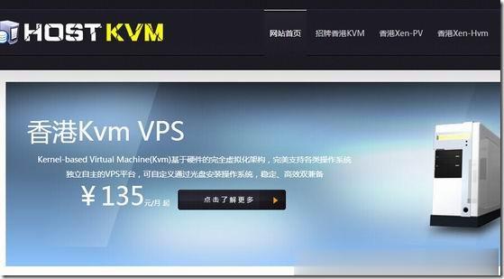
HostKvm:香港国际/韩国KVM夏季7折,2G内存套餐月付5.95美元起
HostKvm是一家成立于2013年的国外主机服务商,主要提供基于KVM架构的VPS主机,可选数据中心包括日本、新加坡、韩国、美国、中国香港等多个地区机房,均为国内直连或优化线路,延迟较低,适合建站或者远程办公等。目前商家发布了夏季特别促销活动,针对香港国际/韩国机房VPS主机提供7折优惠码,其他机房全场8折,优惠后2GB内存套餐月付5.95美元起。下面分别列出几款主机套餐配置信息。套餐:韩国KR...
vpsdime:夏日促销活动,美国达拉斯VPS,2G内存/2核/20gSSD/1T流量,$20/年
vpsdime怎么样?vpsdime是2013年注册的国外VPS主机商,实际上他还有一系列的其他域名站点如Winity.io, Backupsy,Cloudive, Virtora等等,母公司“Nodisto IT”相对来说还是很靠谱了的商家。VPSDime主要提供各种高配低价VPS套餐,其中Linux VPS和存储VPS基于OpenVZ架构,高级VPS基于KVM。VPSDime在上个季度的Low...

CloudCone 新增洛杉矶优化线路 年付17.99美元且简单线路测试
CloudCone 商家在以前的篇幅中也有多次介绍到,这个商家也蛮有意思的。以前一直只有洛杉矶MC机房,而且在功能上和Linode、DO、Vultr一样可以随时删除采用按时计费模式。但是,他们没有学到人家的精华部分,要这样的小时计费,一定要机房多才有优势,否则压根没有多大用途。这不最近CloudCone商家有点小变化,有新人洛杉矶优化线路,具体是什么优化的等会我测试看看线路。内存CPU硬盘流量价格...

dellt110为你推荐
-
蓝瘦香菇被抢注蓝瘦香菇当事人被质疑炒作称没想红 蓝瘦香菇什么意思淘宝门户淘宝社区怎么进?公司网络被攻击网络遭受攻击分为哪几类留学生认证留学生前阶段双认证认证什么内容?同一ip网站同IP的网站互相链接会被K吗?百度关键词分析百度竞价关键词分析需要从哪些数据入手?avtt4.comwww.5c5c.com怎么进入www.mywife.ccMywife-No 00357 MANAMI SAITO种子下载地址有么?求好心人给javbibibibi直播是真的吗www.ijinshan.com好电脑要用什么样的软件