内存储器4内存储器接口
4内存储器接口
The storage capacity of the 1 memory chip: refers to the amount of binary information memory chip can hold, in addressing the product number and storage word digit memory address register said, such as the storage capacity of memory chip 6116 chip is 2K*8, saidtheaddress line 12, theword is storedfor8 digits.Access time of the 2 memory chip is defined as the time required to start the primary memory operation to complete the operation 3 words: "good at low 8 byte value of 16 words in the 8086 system to access the stored in my memory, known as the" aligned "word alignment, for good words, as long as 8086 CPU a bus cycle can be done on the word access
4 parity split: memoryaddress space 1M 8086 bytes in the system is divided into two 512K bytes of memory--"my memory"and"odd memory", even with low memory 8086 8 bit data bus D0 ~ D7 is odd high 8 bit data memory line with 8086 D8~D15 connected to the address bus A1 ~A19 with two banks in the address line A0~ A18 connected to the low address line A0 and bus high allow "BHE*to choose even and odd memory bank. This connection method is called parity".
5 RAM chip on-chip address line and data line number:
(1) 4K * 8 bits: address line 12, data line 8;
(2) 512K * 4 bits: address line 19, data line 4;
(3) 1M * 1 bits: address line 20, data line 1 ;
(4) 2K * 8 bits: address line 11, data line 8.
66116 chip each pin function
6116 is a 2048 x 8 bit static RAM chip with 11 address lines to receive the address signal sent by CPU to select the memory cell to which the CPU is to be accessed. 6116, there are 8 data lines used for reading and writing data in the memory cell. The control signal line 3: CE* chip select signal to select to access the memory chip, CE* pins are usually the same output address decoder is connected to the memory unit and the address decoder input CPU to read and write the high address line. For example, the address of the CPU line is 20 bits, and the memory chip address line 11, address decoder input can be as high as 9 bit address line (A19~A11) ; a write enable signal WE* and an output enable signal OE*, the two signal control signal is written and read to the memory chip, usually the same CPU WR and RD* pins.
72164 chip each pin function
The 2164 is a 64K x 1 bit dynamic RAM chip, 8 address lines,can accept 16 address signals, so it is necessary to use the address multiplexer, the 16bitaddress signal into a8 bit line address and the 8 address to the 2164 row address line. There are 2 lines of data, DIN (input data) and DOUT (output data)that are used to write or read one bit of data information. There are also three control signal lines: RAS* -line address strobe signal. Used to lock 8 bit address; CAS*-column address strobe signal, used to lock the 8 row address; WRITE* - read -write
control signal, used to control the 2164 chip read and write.82732 chip each pin function
The 2732 is a 4K* 8 bit erasable programmable read only memory chip.
There are 12 address lines that can accept the 12 bit address signal from the CPU to select the memory cell to which the CPU is to be accessed. 2732 there are 8 data lines, a data storage unit for reading and writing (in programming work) , there are two control signal lines: line CE* chip allows the chip to select, make it work, allowing the output line OE* is used to output data to the data on the line, only when the two control line at the same time. Effective, to read data from the output end, the readout condition; in programming, OE* programming power line connection VPP=21V, CE* connected to a 50ms active low pulse TTL programming, each such a negative pulse control write a 8 bit data to address a.
9 how many RAM chips are needed in the storage system using the following chips and how many bits of address are needed to decode the off chip address. The system is a 20 bit address line and uses full decoding
(1) a storage system consisting of 512 * 4 bit RAM 16KB:Requires 16KB/512*4=64; the outer address decoding requires 11 bit address lines.
(2) a storage system consisting of 1024 * 1 bit RAM 128KB:
128KB/ lK*8 = 1024 is required; 10 bit address line is needed for decoding of out of chip address;
(3) 2K * 4 bit RAM constitute the storage system of 64KB:Requires 64KB/2K* 2=64; 9 bit address lines are required for decoding of out of chip addresses.
(4) 64K * L bit RAM constitute the storage system of 256KB:We need 256KB / 64K * 8 bits = 32 pieces, and the out of chip address needs 4 bit address lines.
10 what are the memory bars and what are the advantages of using memory?
Memory is a small card appears in the form of memory storage products, a plurality of memory chips are mounted on the printed circuit boardof a strip on the 30, 72 or 168 pinprinting plate on the long side, the memory can be inserted on the motherboard memory slot. The advantage of using memory is that it is easy to install, easy to change and easy to add or expand memory capacity.
Eleven
JustHost:俄罗斯/新西伯利亚vps,512MB内存/5GB空间/不限流量/200Mbps/KVM/自由更换IP,$1.57/月
justhost怎么样?justhost是一家俄罗斯主机商,2006年成立,提供各种主机服务,vps基于kvm,有HDD和SSD硬盘两种,特色是200Mbps不限流量(之前是100Mbps,现在升级为200Mbps)。下面是HDD硬盘的KVM VPS,性价比最高,此外还有SSD硬盘的KVM VPS,价格略高。支持Paypal付款。国内建议选择新西伯利亚或者莫斯科DataLine。支持Paypal付...

Sharktech10Gbps带宽,不限制流量,自带5个IPv4,100G防御
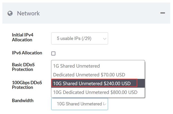
Sharktech荷兰10G带宽的独立服务器月付319美元起,10Gbps共享带宽,不限制流量,自带5个IPv4,免费60Gbps的 DDoS防御,可加到100G防御。CPU内存HDD价格购买地址E3-1270v216G2T$319/月链接E3-1270v516G2T$329/月链接2*E5-2670v232G2T$389/月链接2*E5-2678v364G2T$409/月链接这里我们需要注意,默...

MOACK:韩国服务器/双E5-2450L/8GB内存/1T硬盘/10M不限流量,$59.00/月
Moack怎么样?Moack(蘑菇主机)是一家成立于2016年的商家,据说是国人和韩国合资开办的主机商家,目前主要销售独立服务器,机房位于韩国MOACK机房,网络接入了kt/lg/kinx三条线路,目前到中国大陆的速度非常好,国内Ping值平均在45MS左右,而且商家的套餐比较便宜,针对国人有很多活动。不过目前如果购买机器如需现场处理,由于COVID-19越来越严重,MOACK办公楼里的人也被感染...

-
虚拟空间购买购买虚拟空间要数据库和不要有什么区别?独立ip空间独立IP的空间有什么好处美国虚拟空间请问租用美国虚拟空间,需不需要遵守美国的法律?英文域名求好听的个性英语域名?国内ip代理找一个好用的国内电信IP代理?me域名.me域名和com的价值对比,懂的告诉我呀香港虚拟空间最好的香港虚拟主机是哪家?香港虚拟空间请大哥帮个忙,介绍可靠的香港虚拟主机?100m网站空间网站空间100M指多大网站空间免备案想买一个网站空间,大家给推荐个稳定的,速度的,免备案的?