extended19ise.com
19ise.com 时间:2021-03-20 阅读:()
2008SemiconductorComponentsIndustries,LLC.
PublicationOrderNumber:December-2017,Rev.
2FSA642/DFSA642—Low-Power,Three-Port,High-SpeedMIPISwitchFSA642Low-Power,Three-Port,High-SpeedMIPISwitchFeaturesLowOnCapacitance:7.
0pFTypicalLowOnResistance:7.
0TypicalWide-3dbBandwidth:1GHzTypical24-LeadUMLP(2.
5x3.
4mm)Package8kVESDRating;>16kVPower/GNDESDRatingApplicationsDualCameraApplicationsforCellPhonesDualLCDApplicationsforCellPhones,DigitalCameraDisplays,andViewfindersDescriptionTheFSA642isabi-directional,low-power,high-speedanalogswitch.
Thepinoutisdesignedtoeasedifferentialsignallayoutandisconfiguredasatriple-pole,double-throwswitch(TPDT).
TheFSA642isoptimizedforswitchingbetweentwoMIPIdevices,suchascamerasorLCDdisplaysandon-boardMultimediaApplicationProcessors(MAP).
TheFSA642iscompatiblewiththerequirementsofMobileIndustryProcessorInterface(MIPI).
Thelow-capacitancedesignallowstheFSA642toswitchsignalsthatexceed500MHzinfrequency.
Superiorchannel-to-channelcrosstalkimmunityminimizesinterferenceandallowsthetransmissionofhigh-speeddifferentialsignalsandsingle-endedsignals,asdescribedbytheMIPIspecification.
OrderingInformationPartNumberTopMarkOperatingTemperatureRangePackageFSA642UMXJG-40to+85°C24-Lead,Quad,UltrathinMoldedLeadlessPackage(UMLP),2.
5x3.
4mmFigure1.
ApplicationBlockDiagramwww.
onsemi.
com2FSA642—Low-Power,Three-Port,High-SpeedMIPISwitchPinConfigurationFigure2.
PinConfiguration(TopThroughView)PinDefinitionsPin#NameDescription1,2CLKP,CLKNClockPath(Common)3,4D1P,D1NDataPath1(Common)5,6D2P,D2NDataPath2(Common)7,24NCNoConnect(Float)8/OEOutputEnable(ActiveLow)9GNDGround10VCCPower11SELSelect(0=A,1=B)12,13DA2N,DA2PDataPath(A2)14,15DA1N,DA1PDataPath(A1)16,17CLKAN,CLKAPClockPath(A)18,19DB2N,DB2PDataPath(2B)20,21DB1P,DB1NDataPath(1B)22,23CLKBP,CLKBN,ClockPath(B)www.
onsemi.
com3FSA642—Low-Power,Three-Port,High-SpeedMIPISwitchFunctionalDiagramFigure3.
FunctionalDiagramTruthTableSEL/OEFunctionDon'tCareHIGHDisconnectLOWLOWD1,D2,CLK=DA1,DA2,CLKAHIGHLOWD1,D2,CLK=DB1,DB2,CLKB(5)D2P(6)D2N(3)D1P(4)D1N(1)CLKP(2)CLKNSwitchControlCLKAP(17)CLKAN(16)DA1P(15)DA1N(14)DA2P(13)DA2N(12)CLKBP(22)CLKBN(23)DB1P(20)DB1N(21)FSA642(10)VCC(9)GND(8)/OE(11)SELDB2P(19)DB2N(18)www.
onsemi.
com4FSA642—Low-Power,Three-Port,High-SpeedMIPISwitchAbsoluteMaximumRatingsStressesexceedingtheabsolutemaximumratingsmaydamagethedevice.
Thedevicemaynotfunctionorbeoperableabovetherecommendedoperatingconditionsandstressingthepartstotheselevelsisnotrecommended.
Inaddition,extendedexposuretostressesabovetherecommendedoperatingconditionsmayaffectdevicereliability.
Theabsolutemaximumratingsarestressratingsonly.
SymbolParameterMin.
Max.
UnitVCCSupplyVoltage-0.
50+5.
25VVCNTRLDCInputVoltage(SEL,/OE)(1)-0.
5VCCVVSWDCSwitchI/OVoltage(1)-0.
5VCC+0.
3VIIKDCInputDiodeCurrent-50mAIOUTDCOutputCurrent50mATSTGStorageTemperature-65+150°CESDHumanBodyModel,JEDEC:JESD22-A114AllPins6.
5kVI/OtoGND8.
0PowertoGND16.
0ChargedDeviceModel,JEDEC:JESD22-C1012.
5Note:1.
Theinputandoutputnegativeratingsmaybeexceedediftheinputandoutputdiodecurrentratingsareobserved.
RecommendedOperatingConditionsTheRecommendedOperatingConditionstabledefinestheconditionsforactualdeviceoperation.
Recommendedoperatingconditionsarespecifiedtoensureoptimalperformancetothedatasheetspecifications.
ONSemiconductordoesnotrecommendexceedingthemordesigningtoAbsoluteMaximumRatings.
SymbolParameterMin.
Max.
UnitVCCSupplyVoltage2.
654.
30VVCNTRLControlInputVoltage(SEL,/OE)(2)0VCCVVSWSwitchI/OVoltage-0.
5VCC-1VTAOperatingTemperature-40+85°CNote:2.
ThecontrolinputmustbeheldHIGHorLOW;itmustnotfloat.
www.
onsemi.
com5FSA642—Low-Power,Three-Port,High-SpeedMIPISwitchDCElectricalCharacteristicsAlltypicalvaluesareTA=25°Cunlessotherwisespecified.
SymbolParameterConditionsVCC(V)TA=-40to+85CUnitsMin.
Typ.
Max.
VIKClampDiodeVoltageIIN=-18mA2.
775-1.
2VIINControlInputLeakageVSW=0to4.
3V4.
3-11AVIHInputVoltageHighVIN=0toVCC2.
650to2.
7751.
3V4.
31.
7VILInputVoltageLowVIN=0toVCC2.
650to2.
7750.
5VIOZOff-StateLeakageA,B=0+0.
3VtoVCC-0.
34.
3-22AICCQuiescentSupplyCurrentVCNTRL=0orVCC,IOUT=04.
31.
0AICCTIncreaseinICCCurrentPerControlVoltageandVCCVCNTRL=1.
8V2.
7751.
5ADCElectricalCharacteristics,Low-SpeedModeAlltypicalvaluesareTA=25°Cunlessotherwisespecified.
SymbolParameterConditionsVCC(V)TA=-40to+85CUnitsMin.
Typ.
Max.
RONLSSwitchOnResistance(3)VSW=1.
2V,ION=-10mA,Figure42.
651014RONLSDeltaRON(4)VSW=1.
2V,ION=-10mA(Intra-pair)2.
650.
65Notes:3.
MeasuredbythevoltagedropbetweenA/BandCLK/Dnpinsattheindicatedcurrentthroughtheswitch.
4.
Guaranteedbycharacterization.
DCElectricalCharacteristics,High-SpeedModeAlltypicalvaluesareTA=25°Cunlessotherwisespecified.
SymbolParameterConditionsVCC(V)TA=-40to+85CUnitsMin.
Typ.
Max.
RONHSSwitchOnResistance(5)VSW=0.
4V,ION=-10mA,Figure42.
657.
09.
5RONHSDeltaRON(6)VSW=0.
4V,ION=-10mA(Intra-pair)2.
650.
65Notes:5.
MeasuredbythevoltagedropbetweenA,B,andDnpinsattheindicatedcurrentthroughtheswitch.
6.
Guaranteedbycharacterization.
www.
onsemi.
com6FSA642—Low-Power,Three-Port,High-SpeedMIPISwitchACElectricalCharacteristicsAllvaluesareatRL=50andRS=50andalltypicalvaluesareVCC=2.
775VatTA=25°Cunlessotherwisespecified.
SymbolParameterConditionsVCC(V)TA=-40Cto+85CUnitsMin.
Typ.
Max.
OIRROffIsolation(7)f=100MHz,RT=50Figure142.
775-35dBXtalkNon-AdjacentChannelCrosstalk(7)f=100MHz,RT=50Figure152.
775-55dBBW-3dbBandwidth(7)CL=0pF,RT=50Figure132.
7751.
0GHztONTurn-OnTimeSEL,/OEtoOutputCL=5pF,VSW=1.
2VFigure6,Figure72.
650to2.
7752037nstOFFTurn-OffTimeSEL,/OEtoOutputCL=5pF,VSW=1.
2VFigure6,Figure72.
650to2.
7751527nstPDPropagationDelay(7)CL=5pFFigure6,Figure82.
7750.
25nstBBMBreak-Before-MakeTimeCL=5pF,VSW1=VSW2=1.
2VFigure122.
650to2.
775358nsNote:7.
Guaranteedbycharacterization.
ACElectricalCharacteristics,High-SpeedAlltypicalvaluesareVCC=2.
775VatTA=25°Cunlessotherwisespecified.
SymbolParameterConditionsTA=-40Cto+85CUnitsMin.
Typ.
Max.
tSK(Part_Part)Channel-to-ChannelSkewAcrossMultipleParts(8,9)VSW=0.
2VdiffPP,CL=5pF4080pstSK(Chl_Chl)Channel-to-ChannelSkewWithinaSinglePart(8)VSW=0.
2VdiffPP,CL=5pF,Figure91530pstSK(Pulse)SkewofOppositeTransitionsintheSameDifferentialChannel(8)VSW=0.
2VdiffPP,CL=5pF1020psNotes:8.
Guaranteedbycharacterization.
9.
AssumesthesameVCCandtemperatureforalldevices.
CapacitanceSymbolParameterConditionsTA=-40Cto+85CUnitsMin.
Typ.
Max.
CINControlPinInputCapacitance(10)VCC=0V1.
5pFCONDn/CLK-OnCapacitance(10)VCC=2.
775V,/OE=0V,f=1MHz,at25°C,Figure116.
07.
09.
0COFFDn/CLKOffCapacitance(10)VCC=2.
775V,/OE=2.
775V,f=1MHz,Figure102.
5Note:10.
Guaranteedbycharacterization.
www.
onsemi.
com7FSA642—Low-Power,Three-Port,High-SpeedMIPISwitchTestDiagramsFigure4.
OnResistanceFigure5.
OffLeakageFigure6.
ACTestCircuitLoadFigure7.
Turn-On/Turn-OffWaveformsFigure8.
PropagationDelay(tRtF–500ps)Figure9.
Channel-to-ChannelSkewFigure10.
ChannelOffCapacitanceFigure11.
ChannelOnCapacitanceRL,RS,andCLarefunctionsoftheapplicationenvironment(seeACTablesforspecificvalues).
CLincludestestfixtureandstraycapacitance.
RLCLDnGNDGNDRSVSelVSWGNDVOUTVOUTDA/Bnwww.
onsemi.
com8FSA642—Low-Power,Three-Port,High-SpeedMIPISwitchTestDiagrams(Continued)Figure12.
Break-Before-MakeIntervalTimingFigure13.
BandwidthFigure14.
ChannelOffIsolationFigure15.
Non-AdjacentChannel-to-ChannelCrosstalkVcc0.
9*VoutVcc/2tBBM0VVOUTInput-VSel0.
9*VouttRISE=2.
5ns90%10%CLHSDnRLDnGNDGNDRSVSelVSW1GNDVOUTVSW2GND--RL,RS,andCLarefunctionsoftheapplicationenvironment(seeACTablesforspecificvalues).
CLincludestestfixtureandstraycapacitance.
www.
onsemi.
com9FSA642—Low-Power,Three-Port,High-SpeedMIPISwitchPhysicalDimensionsFigure16.
24-LeadUMLPPackageProduct-SpecificDimensionsDescriptionNominalValues(mm)DescriptionNominalValues(mm)OverallHeight0.
500LeadLength(23x)0.
4PKGStandoff0.
026LeadLength,Pin1(1x)0.
5LeadThickness0.
152LeadPitch0.
4LeadWidth(24x)0.
200BodyLength(X)3.
4BodyWidth(Y)2.
5www.
onsemi.
com10FSA642—Low-Power,Three-Port,High-SpeedMIPISwitchFigure17.
TapeandReelPackingSpecification,page1www.
onsemi.
com11FSA642—Low-Power,Three-Port,High-SpeedMIPISwitchFigure18.
TapeandReelPackingSpecification,page2www.
onsemi.
com12FSA642—Low-Power,Three-Port,High-SpeedMIPISwitchONSemiconductorandtheONSemiconductorlogoaretrademarksofSemiconductorComponentsIndustries,LLCdbaONSemiconductororitssubsidiariesintheUnitedStatesand/orothercountries.
ONSemiconductorownstherightstoanumberofpatents,trademarks,copyrights,tradesecrets,andotherintellectualproperty.
AlistingofONSemiconductor'sproduct/patentcoveragemaybeaccessedatwww.
onsemi.
com/site/pdf/Patent-Marking.
pdf.
ONSemiconductorreservestherighttomakechangeswithoutfurthernoticetoanyproductsherein.
ONSemiconductormakesnowarranty,representationorguaranteeregardingthesuitabilityofitsproductsforanyparticularpurpose,nordoesONSemiconductorassumeanyliabilityarisingoutoftheapplicationoruseofanyproductorcircuit,andspecificallydisclaimsanyandallliability,includingwithoutlimitationspecial,consequentialorincidentaldamages.
BuyerisresponsibleforitsproductsandapplicationsusingONSemiconductorproducts,includingcompliancewithalllaws,regulationsandsafetyrequirementsorstandards,regardlessofanysupportorapplicationsinformationprovidedbyONSemiconductor.
"Typical"parameterswhichmaybeprovidedinONSemiconductordatasheetsand/orspecificationscananddovaryindifferentapplicationsandactualperformancemayvaryovertime.
Alloperatingparameters,including"Typicals"mustbevalidatedforeachcustomerapplicationbycustomer'stechnicalexperts.
ONSemiconductordoesnotconveyanylicenseunderitspatentrightsnortherightsofothers.
ONSemiconductorproductsarenotdesigned,intended,orauthorizedforuseasacriticalcomponentinlifesupportsystemsoranyFDAClass3medicaldevicesormedicaldeviceswithasameorsimilarclassificationinaforeignjurisdictionoranydevicesintendedforimplantationinthehumanbody.
ShouldBuyerpurchaseoruseONSemiconductorproductsforanysuchunintendedorunauthorizedapplication,BuyershallindemnifyandholdONSemiconductoranditsofficers,employees,subsidiaries,affiliates,anddistributorsharmlessagainstallclaims,costs,damages,andexpenses,andreasonableattorneyfeesarisingoutof,directlyorindirectly,anyclaimofpersonalinjuryordeathassociatedwithsuchunintendedorunauthorizeduse,evenifsuchclaimallegesthatONSemiconductorwasnegligentregardingthedesignormanufactureofthepart.
ONSemiconductorisanEqualOpportunity/AffirmativeActionEmployer.
Thisliteratureissubjecttoallapplicablecopyrightlawsandisnotforresaleinanymanner.
PUBLICATIONORDERINGINFORMATIONLITERATUREFULFILLMENT:LiteratureDistributionCenterforONSemiconductor19521E.
32ndPkwy,Aurora,Colorado80011USAPhone:303-675-2175or800-344-3860TollFreeUSA/CanadaFax:303-675-2176or800-344-3867TollFreeUSA/CanadaEmail:orderlit@onsemi.
comN.
AmericanTechnicalSupport:800-282-9855TollFreeUSA/Canada.
Europe,MiddleEastandAfricaTechnicalSupport:Phone:421337902910JapanCustomerFocusCenterPhone:81-3-5817-1050ONSemiconductorWebsite:www.
onsemi.
comOrderLiterature:http://www.
onsemi.
com/orderlitForadditionalinformation,pleasecontactyourlocalSalesRepresentative
- extended19ise.com相关文档
- Progress19ise.com
- grade19ise.com
- nxp19ise.com
- Yearend19ise.com
- devices19ise.com
- influence19ise.com
A400互联37.8元/季,香港节点cn2,cmi线路云服务器,1核/1G/10M/300G
A400互联怎么样?A400互联是一家成立于2020年的商家,A400互联是云服务器网(yuntue.com)首次发布的云主机商家。本次A400互联给大家带来的是,全新上线的香港节点,cmi+cn2线路,全场香港产品7折优惠,优惠码0711,A400互联,只为给你提供更快,更稳,更实惠的套餐,香港节点上线cn2+cmi线路云服务器,37.8元/季/1H/1G/10M/300G,云上日子,你我共享。...

白丝云-美国圣何塞4837/德国4837大带宽/美西9929,26元/月起
官方网站:点击访问白丝云官网活动方案:一、KVM虚拟化套餐A1核心 512MB内存 10G SSD硬盘 800G流量 2560Mbps带宽159.99一年 26一月套餐B1核心 512MB内存 10G SSD硬盘 2000G流量 2560Mbps带宽299.99一年 52一月套餐...
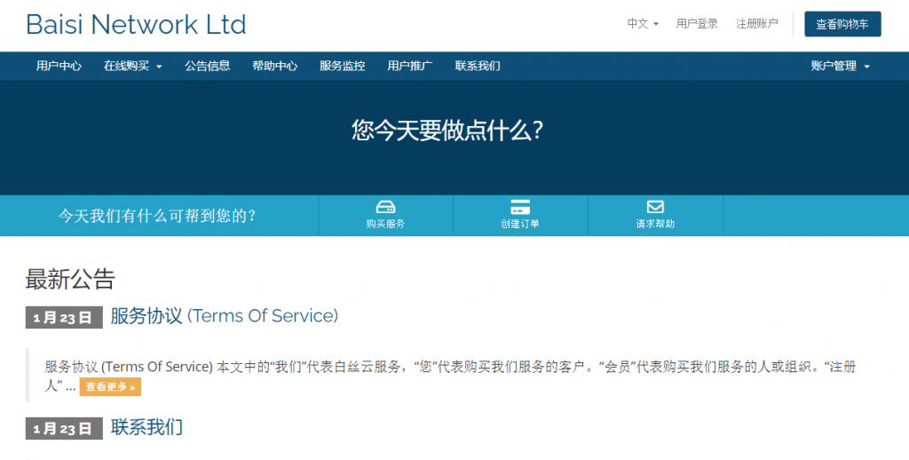
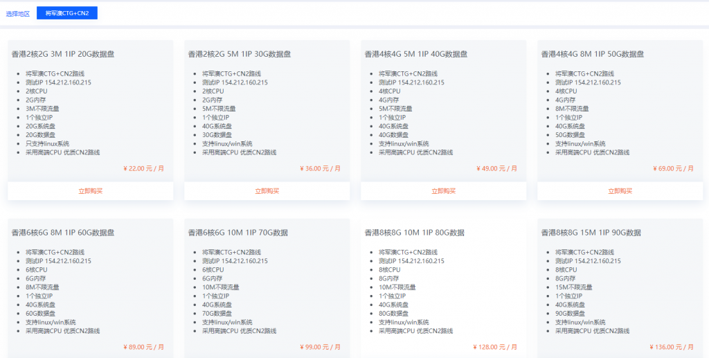
美得云(20元)香港特价将军澳CTG+CN2云服务器
美得云成立于2021年,是一家云产品管理服务商(cloud)专业提供云计算服务、DDOS防护、网络安全服务、国内海外数据中心托管租用等业务、20000+用户的选择,43800+小时稳定运行香港特价将军澳CTG+CN2云服务器、采用高端CPU 优质CN2路线 SDD硬盘。香港CTG+CN22核2G3M20G数据盘25元点击购买香港CTG+CN22核2G5M30G数据盘39元点击购买香港CTG+CN...
19ise.com为你推荐
-
微信回应封杀钉钉微信大封杀什么时候结束微信回应封杀钉钉微信发过来的钉钉链接打不开?bbs.99nets.com怎么把电脑的IP设置和路由器一个网段丑福晋爱新觉罗.允禄真正的福晋是谁?他真的是一个残酷,噬血但很专情的一个人吗?百度关键词工具常见的关键词挖掘工具有哪些www.119mm.comwww.993mm+com精品集!www.gegeshe.com《我的电台fm》 she网址是多少?www.k8k8.com谁能给我几个街污网站我去自己学www.diediao.com谁知道台湾的拼音怎么拼啊?有具体的对照表最好!www.mfav.org手机登录WWW.brcbc.org 能注册么